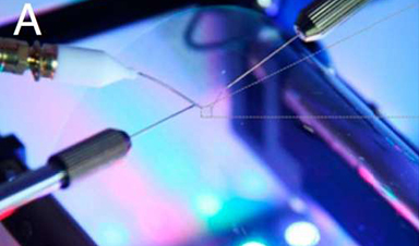
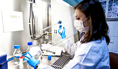
From phys.org:
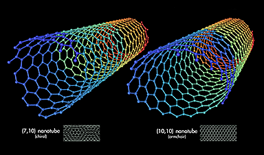
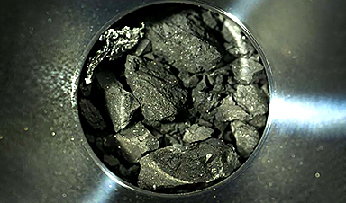
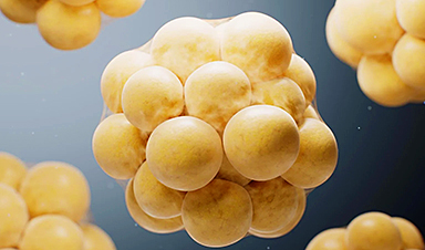
Researchers may have found a “sweet spot” for organic electronics by fabricating a new 2D semiconducting polymer-blended nanonetwork material that simultaneously achieves excellent charge mobility, high flexibility, and nearly 100% optical transparency—a combination of properties that has so far been elusive for semiconducting materials. According to the researchers, the nanonetwork is the first truly colorless, bendable semiconducting material, as demonstrated by the fabrication of field-effect transistors with integrated LEDs.
The researchers, led by Kwanghee Lee, a professor at the Gwangju Institute of Science and Technology in South Korea, have published a paper on the new material in the Proceedings of the National Academy of Sciences.
“So far, there has been no semiconducting material that simultaneously achieves excellent optical transparency, high charge-carrier mobility, and real flexibility,” coauthor Kilho Yu at the Gwangju Institute of Science and Technology told Phys.org. “Metal oxides, such as ZnO and IGZO, have excellent transparency and high mobility, but they are brittle and show poor mobility if not treated with high-temperature (>200 °C) processes, which are not desirable for fabrication on flexible substrates. General semiconducting polymers are flexible, but show poor mobility without complex processes and are not very transparent because of their high optical absorption coefficient.”
Image Credit: Yu et al. ©2016 PNAS
Recent News
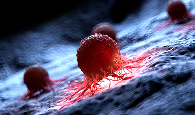
UCLA Scientists Uncover a “Hidden Weakness” in Some of the World’s Deadliest Cancers
A new study has uncovered an unexpected vulnerability in some of the deadliest cancers. Researchers at UCLA have identified a previously hidden weakness in some of the most aggressive cancers, pointing [...]
AI-designed universal coronavirus vaccine clears first human trial
Key Takeaways Super-Antigen Technology: Uses AI and machine learning to analyze viral genomes, creating a single vaccine that targets essential features across entire virus families, including coronaviruses and Ebola. [...]

Researchers Discover a Hidden Vitamin D Problem That Persists Year-Round
A new study suggests that some groups may not experience the expected seasonal boost in vitamin D levels, even during the sunniest months of the year. Many people assume [...]
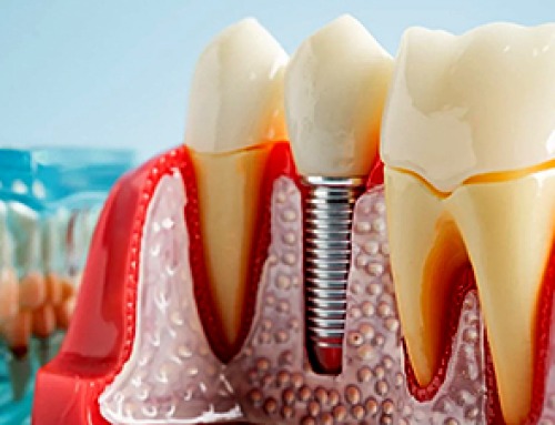
Researchers Solve the Mystery Behind a Billion-Dollar Dental Implant Disease
Researchers have uncovered why a common and costly dental implant infection often resists antibiotics. Dental implants have helped tens of millions of people regain a full set of stable, [...]
Nanoparticles inspired by lung fluid improve therapies targeting respiratory system
The CIC biomaGUNE Center for Cooperative Research in Biomaterials has developed pulmonary surfactant nanoparticles (the blend of lipids and proteins that line the alveoli and [...]
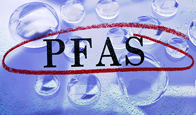
Scientists Finally Uncover How a “Forever Chemical” Causes Birth Defects
PFDA, a PFAS “forever chemical,” can cause craniofacial birth defects by disrupting retinoic acid regulation during fetal development, revealing the first clear molecular mechanism behind the link. Researchers have long linked [...]
Scientists Have Discovered These Deadly Parasites Are Secretly Swapping DNA
Leishmania parasites appear to evolve through widespread genetic exchange, reshaping assumptions about how they adapt and spread. A parasite long thought to spread mostly by cloning itself may be [...]
Stanford’s Revolutionary New Microscope Reveals Living Cells in Stunning Detail
Stanford researchers have developed a microscope that can show how nanostructures interact inside living cells at the highest resolution achieved so far. The view into living cells just got [...]
What Bundibugyo Ebola vaccines and treatments are under development
By Mariam Sunny and Jennifer Rigby May 29 (Reuters) – Global health authorities are racing to identify medical options to help contain an Ebola outbreak in eastern Democratic Republic [...]
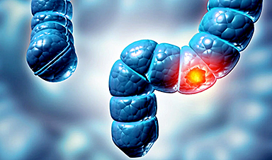
Why More People in Their 30s Are Suddenly Getting Colon Cancer
A major Swiss study found that colorectal cancer is becoming increasingly common in adults under 50, even as rates decline in older age groups. Researchers in Switzerland have identified [...]
Researchers Compare MS Models to Human Tissue in Search for Better Therapies
Researchers identified key differences between two widely used multiple sclerosis models, showing how each can better study myelin damage, immune responses, and repair. The findings may improve efforts to [...]
Scientists Discover Genetic “Off Switch” That Supercharges CAR T Cells Against Cancer
A new study reveals a possible way to make CAR T-cell therapy more durable and effective by targeting a single gene-regulating protein. CAR T-cell therapy is widely seen as [...]
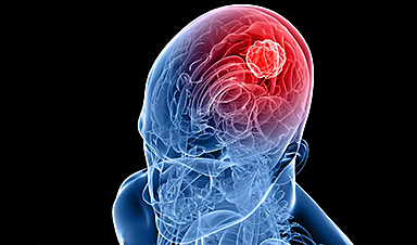
New Vitamin B12-Based Therapy Could Change How Brain Cancer Is Treated
Researchers have identified a vitamin B12–based compound that appears capable of crossing the blood–brain barrier and selectively accumulating in glioblastoma tissue. For decades, one of the biggest problems in [...]

Simple Fiber Supplement Cuts Knee Arthritis Pain in Just 6 Weeks, Study Finds
A daily inulin supplement may help reduce knee osteoarthritis pain while revealing a possible link between gut health, muscle function, and pain sensitivity. For millions of people living with [...]
This Common Vitamin May Help Stop Prediabetes From Turning Into Diabetes
Vitamin D may help prevent type 2 diabetes in people with specific genetic variations, offering a possible path toward personalized diabetes prevention. More than 40% of U.S. adults have [...]

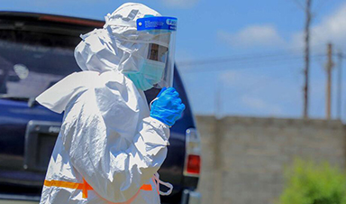
Ebola, hantavirus: Is the world prepared for the next pandemic?
Funding cuts to health research and a growing antivaccine movement are making it harder than ever to respond to viruses. The World Health Organization (WHO) has declared that an [...]

May 2026 Healthcare News and Trends: Market Signals That Matter
Artificial intelligence is dominating headlines, telehealth has settled into a new normal, and digital health continues to promise transformation. However, much of what is being discussed in healthcare today [...]
Scientists Rewire Donor Stem Cells To Outsmart Aggressive Blood Cancers
Researchers have tested a gene-edited stem cell transplant designed to shield healthy blood-forming cells from powerful cancer-targeting immunotherapies. For patients with highly aggressive blood cancers, stem cell transplantation can [...]
Recent Digital Health Trends, Insights and News – May 2026
Last month marked continued progress as digital health moves into its next phase — from AI expanding into drug discovery and core infrastructure to new federal pathways accelerating device [...]
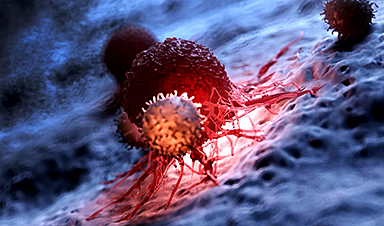
Cancer Mystery Solved: Scientists Discover How Melanoma Becomes “Immortal”
Scientists have uncovered a previously overlooked mechanism that may help melanoma cells become effectively “immortal.” Cancer cells face a major problem before they can become deadly: They have to [...]
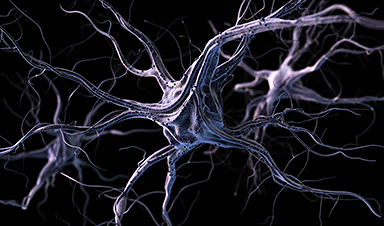
How Visual Neurons Organize Thousands of Synaptic Inputs
Summary: A new study uncovered the organizational rules that determine how neurons in the primary visual cortex process information. By imaging both the cell bodies (soma) and the individual [...]
Scientists Just Found a Surprising Way To Destroy “Forever Chemicals”
Scientists have uncovered a new mechanism that may help break down highly persistent PFAS pollutants. PFAS have earned the nickname “forever chemicals” for a reason. These industrial compounds are [...]
Scientists Discover Cheap Material That Kills Deadly Superbugs
A new sulfur-rich antimicrobial polymer shows strong effectiveness against fungal and bacterial pathogens and may offer an affordable solution to antimicrobial resistance. Antimicrobial resistance is creating growing challenges for [...]

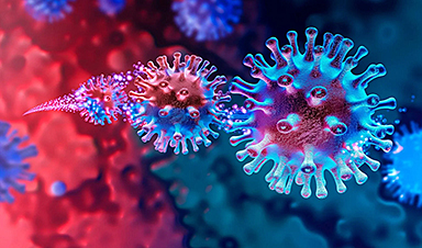
What to Know About Cicada, or BA.3.2, the Latest SARS-CoV-2 Variant Under Monitoring
Like periodical cicadas, the insects for which it is nicknamed, SARS-CoV-2 Omicron subvariant BA.3.2 is only just beginning to emerge after lying low for an extended period since it [...]
Scientists Say This Simple Supplement May Actually Reverse Heart Disease
Scientists in Japan say a common supplement may actually help “unclog” certain diseased heart arteries from the inside out. A simple food supplement sold in Japan may have helped [...]

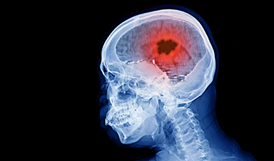
New breakthrough against radiation: Korean Scientists create revolutionary shield with nanotechnology
Korean Scientists develop new nanotechnology material capable of reducing radiation impacts in space missions, hospitals, and power plants. The search for more efficient protection technologies in extreme environments has [...]
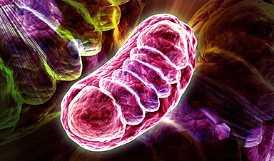
Scientists Just Discovered the Hidden Trick That Keeps Your Cells Alive
A strange bead-like motion inside cells may be the secret to keeping their DNA—and health—in balance. Mitochondria are often described as the power plants of the cell because they [...]

Scientists Discover Stem Cells That Could Regrow Teeth and Bone
Scientists just uncovered the cellular “blueprint” that could one day let us regrow real teeth. Researchers at Science Tokyo have uncovered two distinct stem cell lineages that play a [...]
Scientists Uncover Fatal Weakness in “Zombie Cells” Linked to Cancer
A newly identified weakness in “zombie” cells may open the door to more precise cancer treatments by turning their own survival strategy against them. A new class of drugs [...]

Bowel and Ovarian Cancers Are Dramatically Rising in Young Adults, Scientists Aren’t Sure Why
Cancer incidence is increasing, especially among younger adults, and current risk factors don’t fully account for the trend. Scientists suggest other underlying causes may be contributing. Cancer patterns in [...]
New Immune Pathway Could Supercharge mRNA Cancer Vaccines
A surprising backup system in the immune response to mRNA vaccines may hold the key to more effective cancer treatments. The arrival of mRNA vaccines against SARS-CoV-2 in 2020 marked a [...]
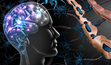
Scientists Discover “Molecular Switch” That Fuels Alzheimer’s Brain Inflammation
A newly identified trigger of brain inflammation could offer a fresh target for slowing Alzheimer’s progression. The brain has its own built-in immune system that identifies threats and responds to them. [...]
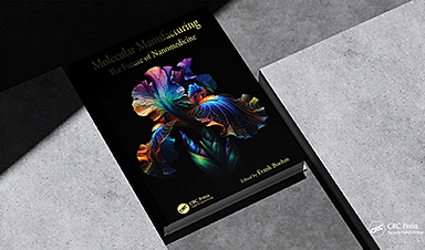
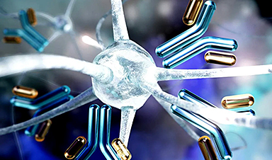
Molecular Manufacturing: The Future of Nanomedicine – New book from NanoappsMedical Inc.
This book explores the revolutionary potential of atomically precise manufacturing technologies to transform global healthcare, as well as practically every other sector across society. This forward-thinking volume examines how [...]
Forgotten Medicinal Plant Shows Promise in Fighting Dangerous Superbugs
A traditional medicinal plant, tormentil, shows promise against antibiotic-resistant bacteria in laboratory tests. Its compounds work by limiting bacterial growth and boosting antibiotic performance. Before the development of modern [...]
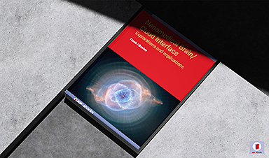
NanoMedical Brain/Cloud Interface – Explorations and Implications. A new book from Frank Boehm
New book from Frank Boehm, NanoappsMedical Inc Founder: This book explores the future hypothetical possibility that the cerebral cortex of the human brain might be seamlessly, safely, and securely [...]

New Research Finds Shocking Link Between Chili Peppers and Cancer
If you love spicy food, you are not alone. But scientists are taking a closer look at whether eating a lot of chili peppers could affect your cancer risk. [...]
New book from Nanoappsmedical Inc. – Global Health Care Equivalency
A new book by Frank Boehm, NanoappsMedical Inc. Founder. This groundbreaking volume explores the vision of a Global Health Care Equivalency (GHCE) system powered by artificial intelligence and quantum [...]
Scientists Create “Neurobots” – Living Machines With Their Own Nervous Systems
Neurobots—xenobots with neurons—show self-organized nervous systems and enhanced behaviors, revealing new insights into how biology builds functional structures. In 2020, researchers at Tufts University developed tiny living structures known as xenobots using [...]
Our books now available worldwide!
Online Sellers other than Amazon, Routledge, and IOPP Indigo Global Health Care Equivalency in the Age of Nanotechnology, Nanomedicine and Artifcial Intelligence Global Health Care Equivalency In The Age [...]

Amazonian Chocolate Could Become the Next Superfood, Scientists Say
New research into Amazonian cocoa reveals that its value may extend beyond flavor alone. Chocolate from the Amazon is already known worldwide for its distinctive taste, but new research [...]
Nanobody repairs misfolded CFTR inside cells, boosting function in cystic fibrosis
A tiny antibody component could fundamentally transform the treatment of cystic fibrosis: For the first time, researchers have succeeded in developing a so-called nanobody that penetrates directly into human [...]
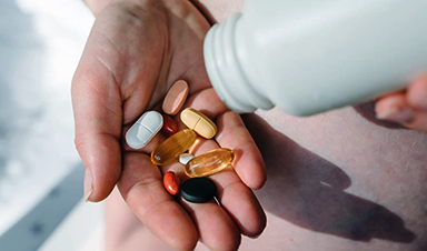
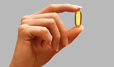
20-Year Study Finds Daily Multivitamins Don’t Extend Lifespan
A large, decades-long study of over 390,000 U.S. adults challenges a widespread assumption about daily multivitamins. Multivitamins are a daily habit for millions of Americans, often taken with the [...]
Novel Investment Paradigms for Regenerative Healthcare Ecosystems
Introduction The transition toward regenerative healthcare ecosystems—anchored in wellness optimization, disease prevention, eradication strategies, and healthy longevity—necessitates a structural reconfiguration of capital architectures, governance models, and incentive design. Regenerative [...]
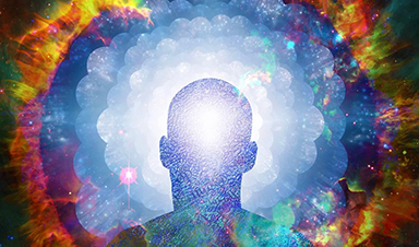
What If Consciousness Exists Beyond Your Brain
Scientists still don’t know how consciousness emerges from the brain. New ideas suggest it may not emerge at all, but instead be a basic feature of reality. Is consciousness [...]
Scientists Discover Way To Treat Lung Cancer and Its Deadly Side Effect Together
A new approach using lipid nanoparticles to deliver genetic material is showing promise in tackling two major challenges in lung cancer at once.Researchers at Oregon State University have designed a new [...]

Saunas Activate Your Immune System
A brief sauna session may quietly mobilize the immune system. A sauna session may do more than raise your heart rate and body temperature. A new study from Finland [...]

Why music from your youth still has such an intense effect years later: A psychological perspective
You're driving, and suddenly a familiar song fills the air. Before you even know it, a wave of emotions comes over you – not just memories, but a deep, [...]
AI to antibody in days: breaking the wet lab bottleneck via high-throughput integration
The role of artificial intelligence (AI) in drug design has fundamentally shifted from a speculative tool to a central pillar of pharmaceutical research and development (R&D). Sino Biological plays [...]
Regenerative Healthcare by Design: Engineering Health-Centric Buildings and Urban Ecosystems
Introduction The next evolution of healthcare will not be confined to hospitals, clinics, or episodic interventions—it will be embedded into the infrastructure of everyday life. Regenerative health ecosystems require [...]
Scientists Warn: Humanity Has Pushed the Planet Past Its Limits
Human population and consumption have surpassed Earth’s limits, increasing risks to climate and global stability. The Earth is already operating beyond its capacity to sustainably support the global population, [...]
Breakthrough Study Reveals Why Damaged Nerves Struggle To Heal
A newly identified molecular mechanism reveals how neurons weigh survival against repair after injury. Scientists at the Icahn School of Medicine at Mount Sinai have identified a molecular switch in neurons [...]
Popular Vitamin B3 Supplements May Help Cancer Cells Survive, Scientists Warn
A new study raises important questions about widely used NAD+ supplements, suggesting that compounds often taken to boost energy and support healthy aging may have unintended consequences in cancer [...]
Scientists Discover Cancer Tumors Are “Addicted” to This Common Antioxidant
Cancer cells may be exploiting a common antioxidant as fuel, revealing a potential weakness that future therapies could target. Cancer cells may be tapping into an unexpected energy source: [...]
Nanotube injector transfers cytoplasmic contents and organelles between living cells safely
Cells are not isolated units; they continuously exchange proteins, genetic material, and even entire organelles with their neighbors. Intercellular transfer influences how tissues develop, respond to stress, and repair [...]
CEO of America’s largest public hospital system is ready to replace radiologists with AI
The chief executive of America’s largest public hospital system says he is prepared to start replacing radiologists with artificial intelligence in some circumstances, once the regulatory landscape catches up. [...]

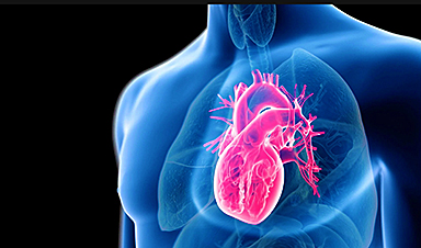
Study finds higher heart disease risk in long COVID patients
People with long COVID are at increased risk of developing cardiovascular disease, according to a new study from Karolinska Institutet published in eClinicalMedicine. The results show that the risk of [...]
The Corona variant Cicada is here – we know that
Online and on social media, reports are piling up about a new Sars-Cov-2 variant that is currently on the rise: BA.3.2, also known as Cicada. That's what it's all [...]
A Simple Blood Test Could Predict Dementia Risk 25 Years Early
A single blood marker may quietly signal dementia risk decades in advance. Scientists at the University of California, San Diego, have identified a blood signal that could forecast dementia risk [...]

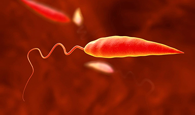
Sperm Get Lost in Space and Scientists Finally Know Why
Having a baby in space may be far more complicated than expected, as new research shows sperm struggle to find their way in microgravity. Starting a family beyond Earth [...]
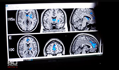
Digital Dementia – Brain fog and disassociation from being chronically online
New medical evidence, featured on 60 Minutes Australia, indicates excessive screen time is causing "digital dementia" in young Australians, with brain scans showing physical shrinkage and damage. Experts warn that [...]
A new, highly mutated COVID variant called ‘Cicada’ is spreading in the US.
BA.3.2, a heavily mutated new COVID-19 variant which may be better able to escape immunity from vaccines or prior infection, is now spreading in the United States. Although COVID [...]

Ancient bacteria strain discovered in ice cave is resistant to some modern antibiotics
In the depths of Scarisoara cave in Romania sits one of the world’s biggest underground glaciers, a monumental slab of ice the size of roughly 40 Olympic swimming pools [...]

Scientists Identify “Good” Bacteria That May Prevent Long COVID
According to the WHO, about 6% of people worldwide who get COVID-19, roughly 400 million people, later develop a long-lasting form of the illness. That shows the condition remains a [...]
RNA Recycling Extends Lifespan
Summary: Researchers discovered a biological “trash disposal” mechanism that directly controls how fast we age. While circular RNA has long been known to accumulate in cells as we get older, [...]
Cancer’s Deadly Paradox: How Tumors Break Their Own DNA To Keep Growing
Cancer’s strongest gene switches push DNA into damaging overdrive, creating repeated breaks and repairs that may fuel tumor evolution while exposing possible therapeutic weak spots. A new study indicates that cancer [...]
Ryugu asteroid samples contain all DNA and RNA building blocks, bolstering origin-of-life theories
All the essential ingredients to make the DNA and RNA underpinning life on Earth have been discovered in samples collected from the asteroid Ryugu, scientists said Monday. The discovery [...]

Is Berberine Really a “Natural Ozempic”?
Often labeled a “natural Ozempic,” berberine is widely discussed as a metabolic aid. Yet research suggests its influence may lie deeper. In recent years, berberine has gained significant attention [...]
Viagra Ingredient Shows Promise for Rare Childhood Brain Disease in Surprising Study
A rare childhood disease with no approved treatment may have an unexpected new therapeutic candidate. Sildenafil, the active ingredient also sold under the brand name Viagra, may help reduce [...]
In a first for China, Neuracle’s implantable brain-computer interface wins approval
In a landmark development, Neuracle Medical Technology has secured the country’s first-ever approval for an implantable brain-computer interface (BCI) system designed to restore hand motor function in patients with [...]
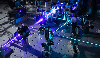
A Cambridge Lab Mistake Reveals a Powerful New Way to Modify Drug Molecules
A surprising lab discovery reveals a light-powered way to tweak complex drugs faster, cleaner, and later in development. Researchers at the University of Cambridge have created a new technique [...]
New book from NanoappsMedical Inc – Molecular Manufacturing: The Future of Nanomedicine
This book explores the revolutionary potential of atomically precise manufacturing technologies to transform global healthcare, as well as practically every other sector across society. This forward-thinking volume examines how [...]
Scientists Discover Simple Saliva Test That Reveals Hidden Diabetes Risk
Researchers have identified a potential new way to assess metabolic health using saliva instead of blood. High insulin levels in the blood, known as hyperinsulinemia, can reveal metabolic problems long before [...]

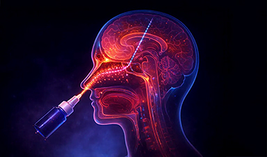
One Nasal Spray Could Protect Against COVID, Flu, Pneumonia, and More
A single nasal spray vaccine may one day protect against viruses, pneumonia, and even allergies. For decades, scientists have dreamed of creating a universal vaccine capable of protecting against [...]
New AI Model Predicts Cancer Spread With Incredible Accuracy
Scientists have developed an AI system that analyzes complex gene-expression signatures to estimate the likelihood that a tumor will spread. Why do some tumors spread throughout the body while [...]
Scientists Discover DNA “Flips” That Supercharge Evolution
In Lake Malawi, hundreds of species of cichlid fish have evolved with astonishing speed, offering scientists a rare opportunity to study how biodiversity arises. Researchers have identified segments of “flipped” DNA that may [...]
Scientists Discover Why Some COVID Survivors Still Can’t Taste Food Years Later
A new study provides the first direct biological evidence explaining why some people continue to experience taste loss long after recovering from COVID-19. Researchers have uncovered specific biological changes in [...]

Catching COVID significantly raises the risk of developing kidney disease, researchers find
Catching Covid significantly raises the risk of developing deadly kidney disease, research has shown. The virus was found to increase the chances that patients will develop the incurable condition [...]
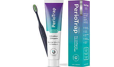
New Toothpaste Stops Gum Disease Without Harming Healthy Bacteria
Researchers have developed a targeted approach to combat periodontitis without disrupting the natural balance of the oral microbiome. The innovation could reshape how gum disease is treated while preserving [...]

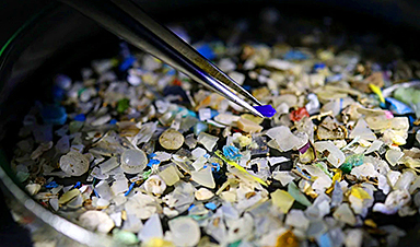
Plastic Without End: Are We Polluting the Planet for Eternity?
The Kunming Montreal Global Biodiversity Framework calls for the elimination of plastic pollution by 2030. If that goal has been clearly set, why have meaningful measures that create real [...]
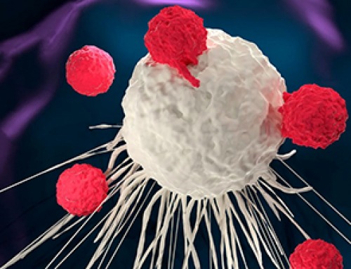
Scientists Rewire Natural Killer Cells To Attack Cancer Faster and Harder
Researchers tested new CAR designs in NK-92 cells and found the modified cells killed tumor cells more effectively, showing stronger anti-cancer activity. Researchers at the Ribeirão Preto Blood Center [...]
New “Cellular” Target Could Transform How We Treat Alzheimer’s Disease
A new study from researchers highlights an unexpected player in Alzheimer’s disease: aging astrocytes. Senescent astrocytes have been identified as a major contributor to Alzheimer’s progression. The cells lose protective functions [...]

Treating a Common Dental Infection… Effects That Extend Far Beyond the Mouth
Successful root canal treatment may help lower inflammation associated with heart disease and improve blood sugar and cholesterol levels. Treating an infected tooth with a successful root canal procedure [...]
Microplastics found in prostate tumors in small study
In a new study, researchers found microplastics deep inside prostate cancer tumors, raising more questions about the role the ubiquitous pollutants play in public health. The findings — which come from [...]
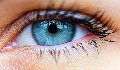
All blue-eyed people have this one thing in common
All Blue-Eyed People Have This One Thing In Common Blue Eyes Aren’t Random—Research Traces Them Back to One Prehistoric Human It sounds like a myth at first — something [...]
Scientists reveal how exercise protects the brain from Alzheimer’s
Researchers at UC San Francisco have identified a biological process that may explain why exercise sharpens thinking and memory. Their findings suggest that physical activity strengthens the brain's built [...]
Deadly Pancreatic Cancer Found To “Wire Itself” Into the Body’s Nerves
A newly discovered link between pancreatic cancer and neural signaling reveals a promising drug target that slows tumor growth by blocking glutamate uptake. Pancreatic cancer is among the most [...]
This Simple Brain Exercise May Protect Against Dementia for 20 Years
A long-running study following thousands of older adults suggests that a relatively brief period of targeted brain training may have effects that last decades. Starting in the late 1990s, [...]
Scientists Crack a 50-Year Tissue Mystery With Major Cancer Implications
Researchers have resolved a 50-year-old scientific mystery by identifying the molecular mechanism that allows tissues to regenerate after severe damage. The discovery could help guide future treatments aimed at [...]

This New Blood Test Can Detect Cancer Before Tumors Appear
A new CRISPR-powered light sensor can detect the faintest whispers of cancer in a single drop of blood. Scientists have created an advanced light-based sensor capable of identifying extremely [...]
Blindness Breakthrough? This Snail Regrows Eyes in 30 Days
A snail that regrows its eyes may hold the genetic clues to restoring human sight. Human eyes are intricate organs that cannot regrow once damaged. Surprisingly, they share key [...]
This Is Why the Same Virus Hits People So Differently
Scientists have mapped how genetics and life experiences leave lasting epigenetic marks on immune cells. The discovery helps explain why people respond so differently to the same infections and [...]
Rejuvenating neurons restores learning and memory in mice
EPFL scientists report that briefly switching on three “reprogramming” genes in a small set of memory-trace neurons restored memory in aged mice and in mouse models of Alzheimer’s disease [...]
New Molecule Blocks Deadliest Brain Cancer at Its Genetic Root
Researchers have identified a molecule that disrupts a critical gene in glioblastoma. Scientists at the UVA Comprehensive Cancer Center say they have found a small molecule that can shut down a [...]
Scientists Finally Solve a 30-Year-Old Cancer Mystery Hidden in Rye Pollen
Nearly 30 years after rye pollen molecules were shown to slow tumor growth in animals, scientists have finally determined their exact three-dimensional structures. Nearly 30 years ago, researchers noticed [...]
How lipid nanoparticles carrying vaccines release their cargo
A study from FAU has shown that lipid nanoparticles restructure their membrane significantly after being absorbed into a cell and ending up in an acidic environment. Vaccines and other [...]
A Virus Designed in the Lab Could Help Defeat Antibiotic Resistance
Scientists can now design bacteria-killing viruses from DNA, opening a faster path to fighting superbugs. Bacteriophages have been used as treatments for bacterial infections for more than a century. Interest [...]
Sleep Deprivation Triggers a Strange Brain Cleanup
When you don’t sleep enough, your brain may clean itself at the exact moment you need it to think. Most people recognize the sensation. After a night of inadequate [...]
Lab-grown corticospinal neurons offer new models for ALS and spinal injuries
Researchers have developed a way to grow a highly specialized subset of brain nerve cells that are involved in motor neuron disease and damaged in spinal injuries. Their study, [...]
Urgent warning over deadly ‘brain swelling’ virus amid fears it could spread globally
Airports across Asia have been put on high alert after India confirmed two cases of the deadly Nipah virus in the state of West Bengal over the past month. Thailand, Nepal [...]

This Vaccine Stops Bird Flu Before It Reaches the Lungs
A new nasal spray vaccine could stop bird flu at the door — blocking infection, reducing spread, and helping head off the next pandemic. Since first appearing in the [...]
These two viruses may become the next public health threats, scientists say
Two emerging pathogens with animal origins—influenza D virus and canine coronavirus—have so far been quietly flying under the radar, but researchers warn conditions are ripe for the viruses to [...]
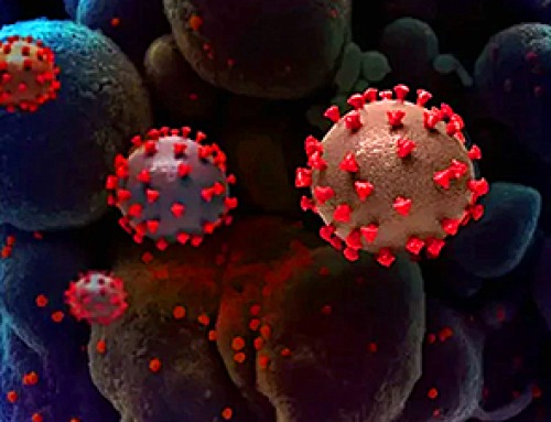
COVID-19 viral fragments shown to target and kill specific immune cells
COVID-19 viral fragments shown to target and kill specific immune cells in UCLA-led study Clues about extreme cases and omicron’s effects come from a cross-disciplinary international research team New [...]
Smaller Than a Grain of Salt: Engineers Create the World’s Tiniest Wireless Brain Implant
A salt-grain-sized neural implant can record and transmit brain activity wirelessly for extended periods. Researchers at Cornell University, working with collaborators, have created an extremely small neural implant that can [...]
Scientists Develop a New Way To See Inside the Human Body Using 3D Color Imaging
A newly developed imaging method blends ultrasound and photoacoustics to capture both tissue structure and blood-vessel function in 3D. By blending two powerful imaging methods, researchers from Caltech and USC have [...]
Brain waves could help paralyzed patients move again
People with spinal cord injuries often lose the ability to move their arms or legs. In many cases, the nerves in the limbs remain healthy, and the brain continues to [...]
Scientists Discover a New “Cleanup Hub” Inside the Human Brain
A newly identified lymphatic drainage pathway along the middle meningeal artery reveals how the human brain clears waste. How does the brain clear away waste? This task is handled [...]
New Drug Slashes Dangerous Blood Fats by Nearly 40% in First Human Trial
Scientists have found a way to fine-tune a central fat-control pathway in the liver, reducing harmful blood triglycerides while preserving beneficial cholesterol functions. When we eat, the body turns [...]
A Simple Brain Scan May Help Restore Movement After Paralysis
A brain cap and smart algorithms may one day help paralyzed patients turn thought into movement—no surgery required. People with spinal cord injuries often experience partial or complete loss [...]
Plant Discovery Could Transform How Medicines Are Made
Scientists have uncovered an unexpected way plants make powerful chemicals, revealing hidden biological connections that could transform how medicines are discovered and produced. Plants produce protective chemicals called alkaloids [...]
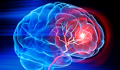
Scientists Develop IV Therapy That Repairs the Brain After Stroke
New nanomaterial passes the blood-brain barrier to reduce damaging inflammation after the most common form of stroke. When someone experiences a stroke, doctors must quickly restore blood flow to [...]
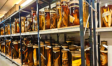
Analyzing Darwin’s specimens without opening 200-year-old jars
Scientists have successfully analyzed Charles Darwin's original specimens from his HMS Beagle voyage (1831 to 1836) to the Galapagos Islands. Remarkably, the specimens have been analyzed without opening their [...]

Scientists discover natural ‘brake’ that could stop harmful inflammation
Researchers at University College London (UCL) have uncovered a key mechanism that helps the body switch off inflammation—a breakthrough that could lead to new treatments for chronic diseases affecting [...]
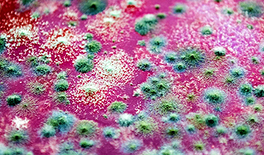
A Forgotten Molecule Could Revive Failing Antifungal Drugs and Save Millions of Lives
Scientists have uncovered a way to make existing antifungal drugs work again against deadly, drug-resistant fungi. Fungal infections claim millions of lives worldwide each year, and current medical treatments [...]
Scientists Trap Thyme’s Healing Power in Tiny Capsules
A new micro-encapsulation breakthrough could turn thyme’s powerful health benefits into safer, smarter nanodoses. Thyme extract is often praised for its wide range of health benefits, giving it a [...]

Scientists Develop Spray-On Powder That Instantly Seals Life-Threatening Wounds
KAIST scientists have created a fast-acting, stable powder hemostat that stops bleeding in one second and could significantly improve survival in combat and emergency medicine. Severe blood loss remains the [...]

Oceans Are Struggling To Absorb Carbon As Microplastics Flood Their Waters
New research points to an unexpected way plastic pollution may be influencing Earth’s climate system. A recent study suggests that microscopic plastic pollution is reducing the ocean’s capacity to [...]
New Book! NanoMedical Brain/Cloud Interface – Explorations and Implications
New book from Frank Boehm, NanoappsMedical Inc Founder: This book explores the future hypothetical possibility that the cerebral cortex of the human brain might be seamlessly, safely, and securely [...]
Global Health Care Equivalency in the Age of Nanotechnology, Nanomedicine and Artificial Intelligence
A new book by Frank Boehm, NanoappsMedical Inc. Founder. This groundbreaking volume explores the vision of a Global Health Care Equivalency (GHCE) system powered by artificial intelligence and quantum [...]
Miller School Researchers Pioneer Nanovanilloid-Based Brain Cooling for Traumatic Injury
A multidisciplinary team at the University of Miami Miller School of Medicine has developed a breakthrough nanodrug platform that may prove beneficial for rapid, targeted therapeutic hypothermia after traumatic brain [...]
COVID-19 still claims more than 100,000 US lives each year
Centers for Disease Control and Prevention researchers report national estimates of 43.6 million COVID-19-associated illnesses and 101,300 deaths in the US during October 2022 to September 2023, plus 33.0 [...]

Leave A Comment