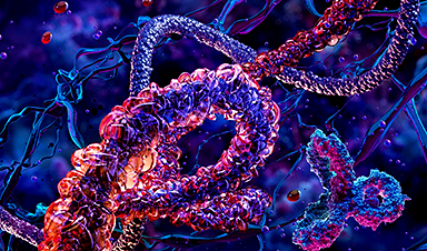
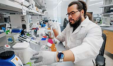
| We can directly see the hidden world of atoms thanks to electron microscopes, first developed in the 1930s. Today, electron microscopes, which use beams of electrons to illuminate and magnify a sample, have become even more sophisticated, allowing scientists to take real-world snapshots of materials with a resolution of less than half the diameter of a hydrogen atom. | |
| Now, scientists at the Department of Energy’s Lawrence Berkeley National Laboratory (Berkeley Lab) are pushing the boundaries of electron microscopy even further through a powerful technique called 4D-STEM, a term that stands for “2D raster of 2D diffraction patterns using scanning transmission electron microscopy.” | |
| Their findings, reported in Nature Communications (“Direct measurement of nanostructural change during in situ deformation of a bulk metallic glass”) and Nature Materials (“Diffraction imaging of nanocrystalline structures in organic semiconductor molecular thin films”), show for the first time how 4D-STEM can provide direct insight into the performance of any material – from strong metallic glass to flexible semiconducting films – by pinpointing specific atomic “neighborhoods” that could compromise a material’s performance, or perhaps have the potential to improve it. |
![]()
Image Credit: Colin Ophus/Berkeley Lab
News This Week
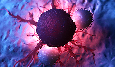
Repurposed drugs could calm the immune system’s response to nanomedicine
An international study led by researchers at the University of Colorado Anschutz Medical Campus has identified a promising strategy to enhance the safety of nanomedicines, advanced therapies often used in cancer and vaccine treatments, [...]

Nano-Enhanced Hydrogel Strategies for Cartilage Repair
A recent article in Engineering describes the development of a protein-based nanocomposite hydrogel designed to deliver two therapeutic agents—dexamethasone (Dex) and kartogenin (KGN)—to support cartilage repair. The hydrogel is engineered to modulate immune responses and promote [...]
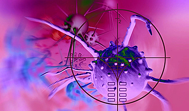
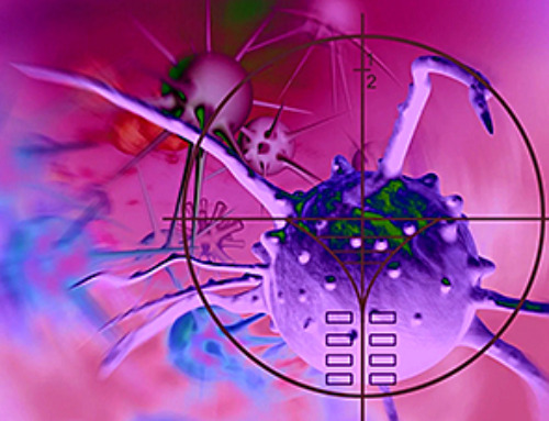
New Cancer Drug Blocks Tumors Without Debilitating Side Effects
A new drug targets RAS-PI3Kα pathways without harmful side effects. It was developed using high-performance computing and AI. A new cancer drug candidate, developed through a collaboration between Lawrence Livermore National Laboratory (LLNL), BridgeBio Oncology [...]

Scientists Are Pretty Close to Replicating the First Thing That Ever Lived
For 400 million years, a leading hypothesis claims, Earth was an “RNA World,” meaning that life must’ve first replicated from RNA before the arrival of proteins and DNA. Unfortunately, scientists have failed to find [...]

Why ‘Peniaphobia’ Is Exploding Among Young People (And Why We Should Be Concerned)
An insidious illness is taking hold among a growing proportion of young people. Little known to the general public, peniaphobia—the fear of becoming poor—is gaining ground among teens and young adults. Discover the causes [...]
Team finds flawed data in recent study relevant to coronavirus antiviral development
The COVID pandemic illustrated how urgently we need antiviral medications capable of treating coronavirus infections. To aid this effort, researchers quickly homed in on part of SARS-CoV-2's molecular structure known as the NiRAN domain—an [...]
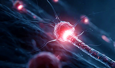
Drug-Coated Neural Implants Reduce Immune Rejection
Summary: A new study shows that coating neural prosthetic implants with the anti-inflammatory drug dexamethasone helps reduce the body’s immune response and scar tissue formation. This strategy enhances the long-term performance and stability of electrodes [...]

Scientists discover cancer-fighting bacteria that ‘soak up’ forever chemicals in the body
A family of healthy bacteria may help 'soak up' toxic forever chemicals in the body, warding off their cancerous effects. Forever chemicals, also known as PFAS (per- and polyfluoroalkyl substances), are toxic chemicals that [...]
Johns Hopkins Researchers Uncover a New Way To Kill Cancer Cells
A new study reveals that blocking ribosomal RNA production rewires cancer cell behavior and could help treat genetically unstable tumors. Researchers at the Johns Hopkins Kimmel Cancer Center and the Department of Radiation Oncology and Molecular [...]
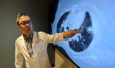
AI matches doctors in mapping lung tumors for radiation therapy
In radiation therapy, precision can save lives. Oncologists must carefully map the size and location of a tumor before delivering high-dose radiation to destroy cancer cells while sparing healthy tissue. But this process, called [...]
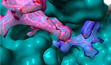
Scientists Finally “See” Key Protein That Controls Inflammation
Researchers used advanced microscopy to uncover important protein structures. For the first time, two important protein structures in the human body are being visualized, thanks in part to cutting-edge technology at the University of [...]

AI tool detects 9 types of dementia from a single brain scan
Mayo Clinic researchers have developed a new artificial intelligence (AI) tool that helps clinicians identify brain activity patterns linked to nine types of dementia, including Alzheimer's disease, using a single, widely available scan—a transformative [...]

Is plastic packaging putting more than just food on your plate?
New research reveals that common food packaging and utensils can shed microscopic plastics into our food, prompting urgent calls for stricter testing and updated regulations to protect public health. Beyond microplastics: The analysis intentionally [...]

Aging Spreads Through the Bloodstream
Summary: New research reveals that aging isn’t just a local cellular process—it can spread throughout the body via the bloodstream. A redox-sensitive protein called ReHMGB1, secreted by senescent cells, was found to trigger aging features [...]
AI and nanomedicine find rare biomarkers for prostrate cancer and atherosclerosis
Imagine a stadium packed with 75,000 fans, all wearing green and white jerseys—except one person in a solid green shirt. Finding that person would be tough. That's how hard it is for scientists to [...]
Are Pesticides Breeding the Next Pandemic? Experts Warn of Fungal Superbugs
Fungicides used in agriculture have been linked to an increase in resistance to antifungal drugs in both humans and animals. Fungal infections are on the rise, and two UC Davis infectious disease experts, Dr. George Thompson [...]