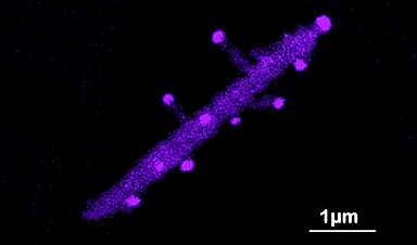
| A research team of Ehime University paved a way to achieve unexplored III-V semiconductor nanostructures. They grew branched GaAs nanowires with a nontoxic Bi element employing characteristic structural modifications correlated with metallic droplets, as well as crystalline defects and orientations. | |
| The finding provides a rational design concept for the creation of semiconductor nanostructures with the concentration of constituents beyond the fundamental limit, making it potentially applicable to novel efficient near-infrared devices and quantum electronics. | |
| Nanowire is a rod-structure with a diameter typically narrower than several hundred nanometers. Due to its size and structure, it exhibits characteristic properties which are not found in larger bulk materials. The study of III-V semiconductor nanowires has attracted much interest in recent decades due to their potential application in nanoscale quantum, photonic, electronic, and energy conversion, and in biological devices, based on their one-dimensional nature and large surface to volume ratio. | |
| The introduction of an epitaxial heterostructure facilitates control of the transport and electronic properties of such devices, showing the potential for realizing integrated systems based on III-V compounds and Si with superior electronic and optical functions. |
| III-V compound semiconductors are one of the highest in mobility and photon-electron conversion efficiency in existence. Among them, GaAs is a representative III-V compound semiconductor, which is utilized for high speed transistors, as well as high-efficiency near-infrared light-emitting diodes, lasers, and solar cells. Optical devices based on III-V GaAs suffer from intrinsic losses related to heat generation. | |
| To circumvent this, the use of dilute bismide GaAsBi alloy with a nontoxic Bi element has recently gained attention because the introduction of Bi suppresses heat generation while increasing electron-light conversion efficiency. Therefore, incorporating dilute bismide GaAsBi alloy into nanowires is a rational approach for developing high-performance optoelectronic nanodevices. | |
| Meanwhile, branched or tree-like nanowires offer an approach to increase structural complexity and enhance the resulting functions which in turn enable the realization of higher dimensionality structures, lateral connectivity, and interconnection between the nanowires. |
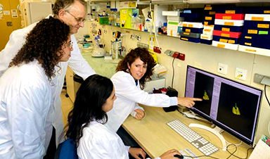
![]()
Image Credit: Ehime University
News This Week
UCLA Scientists Uncover a “Hidden Weakness” in Some of the World’s Deadliest Cancers
A new study has uncovered an unexpected vulnerability in some of the deadliest cancers. Researchers at UCLA have identified a previously hidden weakness in some of the most aggressive cancers, pointing to a possible new way [...]
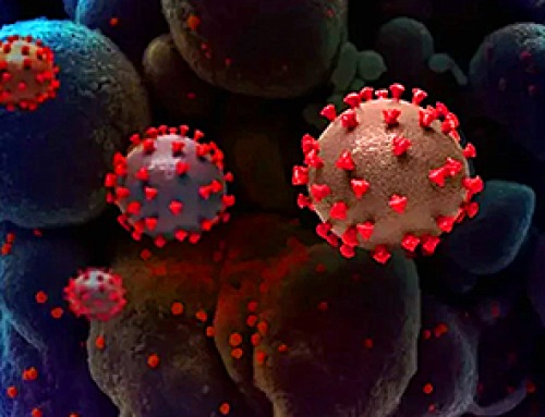
AI-designed universal coronavirus vaccine clears first human trial
Key Takeaways Super-Antigen Technology: Uses AI and machine learning to analyze viral genomes, creating a single vaccine that targets essential features across entire virus families, including coronaviruses and Ebola. Human Trials & Safety: Phase [...]

Researchers Discover a Hidden Vitamin D Problem That Persists Year-Round
A new study suggests that some groups may not experience the expected seasonal boost in vitamin D levels, even during the sunniest months of the year. Many people assume that spending more time outdoors [...]
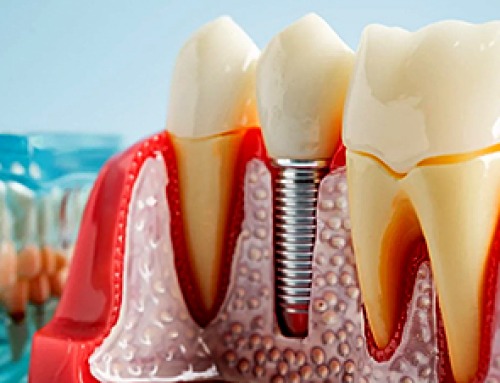
Researchers Solve the Mystery Behind a Billion-Dollar Dental Implant Disease
Researchers have uncovered why a common and costly dental implant infection often resists antibiotics. Dental implants have helped tens of millions of people regain a full set of stable, functional teeth, something traditional dentures [...]
Nanoparticles inspired by lung fluid improve therapies targeting respiratory system
The CIC biomaGUNE Center for Cooperative Research in Biomaterials has developed pulmonary surfactant nanoparticles (the blend of lipids and proteins that line the alveoli and enables breathing), which are encapsulated [...]

Scientists Finally Uncover How a “Forever Chemical” Causes Birth Defects
PFDA, a PFAS “forever chemical,” can cause craniofacial birth defects by disrupting retinoic acid regulation during fetal development, revealing the first clear molecular mechanism behind the link. Researchers have long linked perfluoroalkyl and polyfluoroalkyl substances (PFAS), [...]
Scientists Have Discovered These Deadly Parasites Are Secretly Swapping DNA
Leishmania parasites appear to evolve through widespread genetic exchange, reshaping assumptions about how they adapt and spread. A parasite long thought to spread mostly by cloning itself may be far more genetically dynamic than [...]
Stanford’s Revolutionary New Microscope Reveals Living Cells in Stunning Detail
Stanford researchers have developed a microscope that can show how nanostructures interact inside living cells at the highest resolution achieved so far. The view into living cells just got better. Stanford researchers have merged [...]

What Bundibugyo Ebola vaccines and treatments are under development
By Mariam Sunny and Jennifer Rigby May 29 (Reuters) – Global health authorities are racing to identify medical options to help contain an Ebola outbreak in eastern Democratic Republic of Congo, linked to the [...]
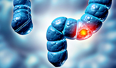
Why More People in Their 30s Are Suddenly Getting Colon Cancer
A major Swiss study found that colorectal cancer is becoming increasingly common in adults under 50, even as rates decline in older age groups. Researchers in Switzerland have identified a concerning trend: while colorectal [...]
Researchers Compare MS Models to Human Tissue in Search for Better Therapies
Researchers identified key differences between two widely used multiple sclerosis models, showing how each can better study myelin damage, immune responses, and repair. The findings may improve efforts to develop treatments that restore lost [...]
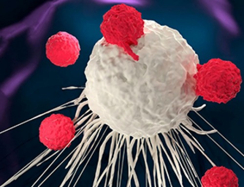
Scientists Discover Genetic “Off Switch” That Supercharges CAR T Cells Against Cancer
A new study reveals a possible way to make CAR T-cell therapy more durable and effective by targeting a single gene-regulating protein. CAR T-cell therapy is widely seen as a breakthrough in personalized cancer [...]
New Vitamin B12-Based Therapy Could Change How Brain Cancer Is Treated
Researchers have identified a vitamin B12–based compound that appears capable of crossing the blood–brain barrier and selectively accumulating in glioblastoma tissue. For decades, one of the biggest problems in brain cancer treatment has had [...]

Simple Fiber Supplement Cuts Knee Arthritis Pain in Just 6 Weeks, Study Finds
A daily inulin supplement may help reduce knee osteoarthritis pain while revealing a possible link between gut health, muscle function, and pain sensitivity. For millions of people living with knee osteoarthritis, managing chronic pain [...]

This Common Vitamin May Help Stop Prediabetes From Turning Into Diabetes
Vitamin D may help prevent type 2 diabetes in people with specific genetic variations, offering a possible path toward personalized diabetes prevention. More than 40% of U.S. adults have prediabetes, a condition in which [...]

Ebola, hantavirus: Is the world prepared for the next pandemic?
Funding cuts to health research and a growing antivaccine movement are making it harder than ever to respond to viruses. The World Health Organization (WHO) has declared that an Ebola outbreak in Uganda and [...]