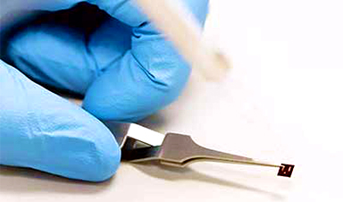
| New methods of arranging silver nanowires make them more durable, shows a study by KAUST. These nanowires form flexible, transparent conductive layers that can be used for improved solar cells, strain sensors and next-generation mobile phones. | |
| Applying nanotechnology in electronic devices requires rigorous testing of individual tiny components to ensure they will stand up to use. Silver nanowires show great promise as connectors that could be arranged in flexible, near-transparent meshes for touchscreens or solar cells, but it is unclear how they will respond to prolonged stresses from bending and carrying current. | |
| Testing the bulk properties of a large sample of nanoparticles is easy, but not completely revelatory. However, adopting transmission electron microscopy (TEM) makes it possible to examine individual nanoparticles. Ph.D. student Nitin Batra andhis supervisor Pedro Da Costa are at the forefront of developing new TEM techniques. This has allowed them to study single silver nanowires in detail (Nanoscale, “Current-induced restructuring in bent silver nanowires”). |
Image Credit: KAUST
News This Week
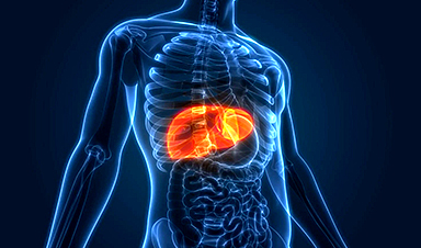
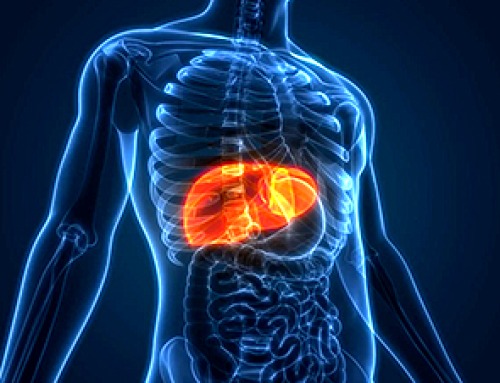
Scientists Create Tiny “Mini Livers” That Could One Day Replace Liver Transplants
Engineered tissue grafts could help perform key liver functions and benefit thousands of people living with liver failure. The liver is one of the body’s hardest-working organs, carrying out hundreds of vital jobs, from [...]
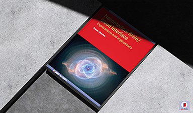
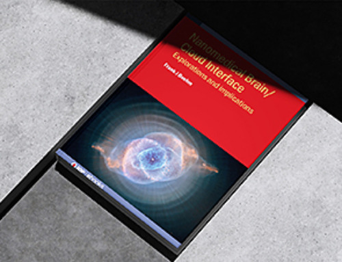
NanoMedical Brain/Cloud Interface – Explorations and Implications. A new book from Frank Boehm
New book from Frank Boehm, NanoappsMedical Inc Founder: This book explores the future hypothetical possibility that the cerebral cortex of the human brain might be seamlessly, safely, and securely connected with the Cloud via [...]
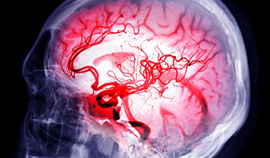
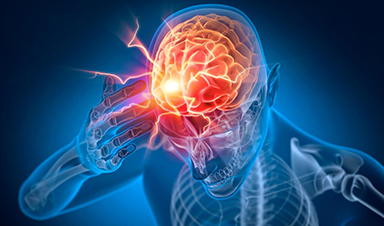
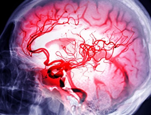
Scientists Discover Surprising Way To Help the Brain Recover After Stroke
A new study suggests that strengthening the body’s natural circadian rhythms may help the brain recover after stroke, even when treatment begins days after the injury. Every year, millions of people survive a stroke, [...]
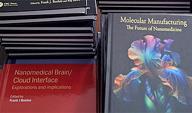
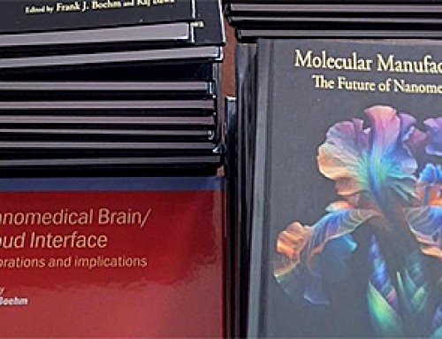
Our books now available worldwide!
Online Sellers other than Amazon, Routledge, and IOPP Indigo Global Health Care Equivalency in the Age of Nanotechnology, Nanomedicine and Artifcial Intelligence Global Health Care Equivalency In The Age Of Nanotechnology, Nanomedicine And Artificial [...]

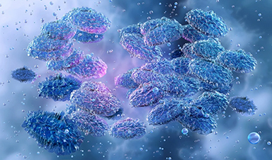
Younger Generations Are Aging Faster – and It May Be Fueling a Surge in Cancer
Younger generations may be aging biologically faster than those before them, and that shift could help explain rising rates of cancer at younger ages. For decades, cancer was viewed largely as a disease of [...]
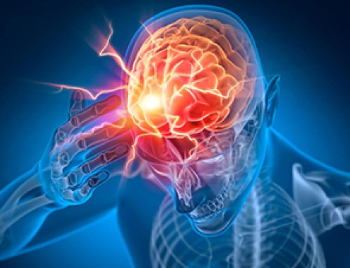
Using Cannabis Could Raise Your Stroke Risk by 37%, Massive Study Reveals
Large-scale evidence suggests cannabis, cocaine, and amphetamines may directly raise stroke risk, including in younger adults. As recreational drug use becomes increasingly common, researchers are uncovering evidence that its health consequences may extend far beyond [...]

Could Vitamin C Be the Secret to Keeping Your Brain Younger?
Lower vitamin C levels were linked to reduced brain volume and weaker neural connectivity in older adults, suggesting a potential connection between nutrition and brain health. Could a common vitamin help preserve the brain [...]
This Deadly Disease Was Wiping Out Humans 5,500 Years Ago
A new study suggests plague was already a deadly threat 5,500 years ago, striking small hunter-gatherer communities long before cities and agriculture emerged. For centuries, plague has been remembered as the disease that devastated [...]


Leave A Comment