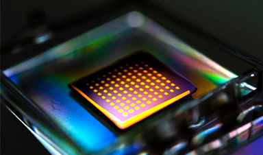
Following the discovery of graphene in 2003, there has been considerable interest in other types of 2D materials. However, splitting a bulk crystal material into 2D flakes for use in electronics has proven hard to achieve on a commercial scale.
Now, scientists in the Department of Mechanical Engineering at MIT have formulated a method to harvest 2-inch diameter wafers of 2D materials in a matter of minutes. They can then be stacked together to create an electronic device in less than an hour.
The method, which they illustrate in a paper reported in the journal Science, could lead to the possibility of commercializing electronic devices based on a range of 2D materials, according to Jeehwan Kim, an associate professor in the Department of Mechanical Engineering, who headed the research.
The paper’s co-first authors are Sang-hoon Bae, who worked on flexible device fabrication, and Jaewoo Shim, who was involved in the stacking of the 2D material monolayers. They are postdocs in Kim’s group.
The co-authors of the paper also included students and postdocs from within Kim’s group, as well as collaborators at Georgia Tech, the University of Texas, Yonsei University in South Korea, and the University of Virginia. Sang-Hoon Bae, Jaewoo Shim, Wei Kong, and Doyoon Lee in Kim’s research group equally contributed to this research.
Image Credit: Peng Lin
News This Week

Scientists Create Tiny “Mini Livers” That Could One Day Replace Liver Transplants
Engineered tissue grafts could help perform key liver functions and benefit thousands of people living with liver failure. The liver is one of the body’s hardest-working organs, carrying out hundreds of vital jobs, from [...]
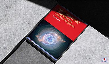
NanoMedical Brain/Cloud Interface – Explorations and Implications. A new book from Frank Boehm
New book from Frank Boehm, NanoappsMedical Inc Founder: This book explores the future hypothetical possibility that the cerebral cortex of the human brain might be seamlessly, safely, and securely connected with the Cloud via [...]

Scientists Discover Surprising Way To Help the Brain Recover After Stroke
A new study suggests that strengthening the body’s natural circadian rhythms may help the brain recover after stroke, even when treatment begins days after the injury. Every year, millions of people survive a stroke, [...]
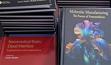
Our books now available worldwide!
Online Sellers other than Amazon, Routledge, and IOPP Indigo Global Health Care Equivalency in the Age of Nanotechnology, Nanomedicine and Artifcial Intelligence Global Health Care Equivalency In The Age Of Nanotechnology, Nanomedicine And Artificial [...]

Younger Generations Are Aging Faster – and It May Be Fueling a Surge in Cancer
Younger generations may be aging biologically faster than those before them, and that shift could help explain rising rates of cancer at younger ages. For decades, cancer was viewed largely as a disease of [...]

Using Cannabis Could Raise Your Stroke Risk by 37%, Massive Study Reveals
Large-scale evidence suggests cannabis, cocaine, and amphetamines may directly raise stroke risk, including in younger adults. As recreational drug use becomes increasingly common, researchers are uncovering evidence that its health consequences may extend far beyond [...]

Could Vitamin C Be the Secret to Keeping Your Brain Younger?
Lower vitamin C levels were linked to reduced brain volume and weaker neural connectivity in older adults, suggesting a potential connection between nutrition and brain health. Could a common vitamin help preserve the brain [...]

This Deadly Disease Was Wiping Out Humans 5,500 Years Ago
A new study suggests plague was already a deadly threat 5,500 years ago, striking small hunter-gatherer communities long before cities and agriculture emerged. For centuries, plague has been remembered as the disease that devastated [...]
China closing in but US leads in biotech quality, commercial reach, survey finds
SAN DIEGO, June 22 (Reuters) - China, which now conducts more clinical drug trials, opens new tab than the U.S., still lags in the quality and commercial reach of its biomedical science, according to a recent survey, opens new [...]
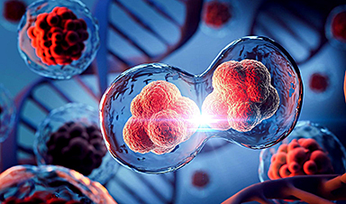
New method generates renewable supply of progenitor immune cells
In a paper published in Cell, a USC Stem Cell-led team reports a new way of generating a renewable and expandable supply of the progenitor cells that give rise to macrophages. These immune cells help [...]
Scientists Just Discovered a Cellular Survival System That Was Never Supposed To Exist
A surprising backup pathway allows cells to make a crucial amino acid when their primary machinery fails. For decades, biologists believed cells had only one way to access a molecule they cannot live without. New [...]
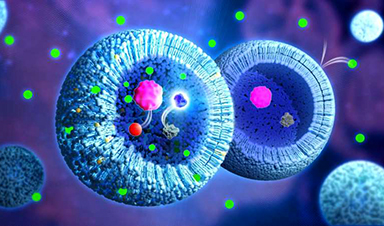
Artificial cells gain porous membranes, enabling lab reactions and drug release
Artificial cells created in the laboratory offer a wide range of potential applications. Until now, however, their membranes—unlike those of real cells—have been virtually impermeable. Researchers at the Max Planck Institute for Polymer Research, [...]

Popular Weight-Loss Drugs Like Ozempic Linked to Lower Breast Cancer Risk
Ozempic and similar weight-loss drugs were linked to a striking 30% reduction in breast cancer risk in a study of more than 110,000 women. Popular weight-loss and diabetes medications such as Ozempic, Wegovy, Mounjaro, [...]

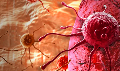
Stanford Scientists Discover Explosive New Type of Immune Cell
Scientists studying the remarkable regenerative abilities of planarian flatworms have uncovered a previously unknown type of immune cell with an unusually destructive defense strategy. What if an immune cell could wipe out nearby threats [...]

Big Pharma-backed SonoThera sounds off with $125M series B for bubble-based genetic delivery
Bay Area biotech SonoThera is bubbling to a clinical boil after raising a $125 million series B with the backing of some of the biggest names in pharma. Vida Ventures led the raise, with the venture [...]

Joint initiative of 5 EU countries calls for ‘unified approach’ to pharma framework amid US drug pricing pressure
With drug pricing pressure building from the U.S., a healthcare-focused consortium of five European countries is calling for a “unified approach” to strengthen Europe’s pharmaceutical framework and access to innovative medicines. Belgium, the Netherlands, [...]


Leave A Comment