| A household microwave oven modified by a Cornell Engineering professor is helping to cook up the next generation of cellphones, computers and other electronics after the invention was shown to overcome a major challenge faced by the semiconductor industry. | |
| The research is detailed in a paper in Applied Physics Letters (“Efficient and stable activation by microwave annealing of nanosheet silicon doped with phosphorus above its solubility limit”). The lead author is James Hwang, a research professor in the Department of Materials Science and Engineering; other Cornell contributors are doctoral student Chandrasekhar Savant and former postdoctoral researcher Mohammed Javad Asadi. |
| Producing the materials that make up transistors and other microchip components is similar to baking in that material ingredients must be mixed together and then heated, among other steps, in order to produce a desired electrical current. For instance, phosphorus is added to silicon and then the mixture is annealed, or heated, to position the phosphorus atoms into the correct place so that they are active in current conduction. | |
| But as microchips continue to shrink, the silicon must be doped, or mixed, with higher concentrations of phosphorus to produce the desired current. Semiconductor manufacturers are now approaching a critical limit in which heating the highly doped materials using traditional methods no longer produces consistently functional semiconductors. | |
| “We need concentrations of phosphorus that are higher than its equilibrium solubility in silicon. That goes against nature,” Hwang said. “The silicon crystal expands, causing immense strain and making it potentially useless for electronics.” | |
| The Taiwan Semiconductor Manufacturing Company (TSMC) had theorized that microwaves could be used to activate the excess dopants, but just like with household microwave ovens that sometimes heat food unevenly, previous microwave annealers produced “standing waves” that prevented consistent dopant activation. So TSMC partnered with Hwang, who modified a microwave oven to selectively control where the standing waves occur. Such precision allows for the proper activation of the dopants without excessive heating or damage of the silicon crystal. | |
| This discovery could be used to produce semiconductor materials and electronics appearing around the year 2025, said Hwang, who has filed two patents for the prototype microwave annealer with postdoctoral researcher Gianluca Fabi. | |
| “A few manufacturers are currently producing semiconductor materials that are 3 nanometers,” Hwang said. “This new microwave approach can potentially enable leading manufacturers such as TSMC and Samsung to scale down to just 2 nanometers.” | |
| The breakthrough could change the geometry of transistors used in microchips. For more than 20 years, transistors have been made to stand up like dorsal fins so that more can be packed on each microchip, but manufacturers have recently begun to experiment with a new architecture in which transistors are stacked horizontally as nanosheets that can further increase the density and control of transistors. The excessively doped materials enabled by microwave annealing would be key to the new architecture. |
News

Drug-Coated Neural Implants Reduce Immune Rejection
Summary: A new study shows that coating neural prosthetic implants with the anti-inflammatory drug dexamethasone helps reduce the body’s immune response and scar tissue formation. This strategy enhances the long-term performance and stability of electrodes [...]

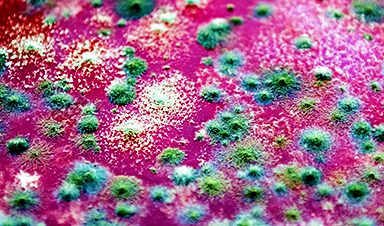
Scientists discover cancer-fighting bacteria that ‘soak up’ forever chemicals in the body
A family of healthy bacteria may help 'soak up' toxic forever chemicals in the body, warding off their cancerous effects. Forever chemicals, also known as PFAS (per- and polyfluoroalkyl substances), are toxic chemicals that [...]
Johns Hopkins Researchers Uncover a New Way To Kill Cancer Cells
A new study reveals that blocking ribosomal RNA production rewires cancer cell behavior and could help treat genetically unstable tumors. Researchers at the Johns Hopkins Kimmel Cancer Center and the Department of Radiation Oncology and Molecular [...]
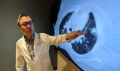
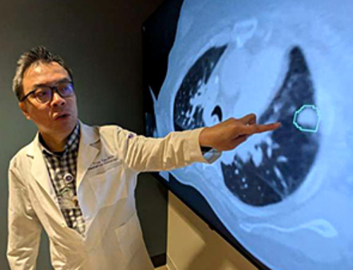
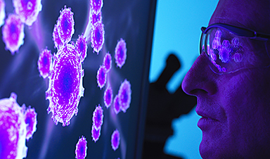
AI matches doctors in mapping lung tumors for radiation therapy
In radiation therapy, precision can save lives. Oncologists must carefully map the size and location of a tumor before delivering high-dose radiation to destroy cancer cells while sparing healthy tissue. But this process, called [...]
Scientists Finally “See” Key Protein That Controls Inflammation
Researchers used advanced microscopy to uncover important protein structures. For the first time, two important protein structures in the human body are being visualized, thanks in part to cutting-edge technology at the University of [...]

AI tool detects 9 types of dementia from a single brain scan
Mayo Clinic researchers have developed a new artificial intelligence (AI) tool that helps clinicians identify brain activity patterns linked to nine types of dementia, including Alzheimer's disease, using a single, widely available scan—a transformative [...]

Is plastic packaging putting more than just food on your plate?
New research reveals that common food packaging and utensils can shed microscopic plastics into our food, prompting urgent calls for stricter testing and updated regulations to protect public health. Beyond microplastics: The analysis intentionally [...]
Aging Spreads Through the Bloodstream
Summary: New research reveals that aging isn’t just a local cellular process—it can spread throughout the body via the bloodstream. A redox-sensitive protein called ReHMGB1, secreted by senescent cells, was found to trigger aging features [...]
AI and nanomedicine find rare biomarkers for prostrate cancer and atherosclerosis
Imagine a stadium packed with 75,000 fans, all wearing green and white jerseys—except one person in a solid green shirt. Finding that person would be tough. That's how hard it is for scientists to [...]
Are Pesticides Breeding the Next Pandemic? Experts Warn of Fungal Superbugs
Fungicides used in agriculture have been linked to an increase in resistance to antifungal drugs in both humans and animals. Fungal infections are on the rise, and two UC Davis infectious disease experts, Dr. George Thompson [...]
Scientists Crack the 500-Million-Year-Old Code That Controls Your Immune System
A collaborative team from Penn Medicine and Penn Engineering has uncovered the mathematical principles behind a 500-million-year-old protein network that determines whether foreign materials are recognized as friend or foe. How does your body [...]
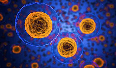
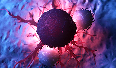
Team discovers how tiny parts of cells stay organized, new insights for blocking cancer growth
A team of international researchers led by scientists at City of Hope provides the most thorough account yet of an elusive target for cancer treatment. Published in Science Advances, the study suggests a complex signaling [...]
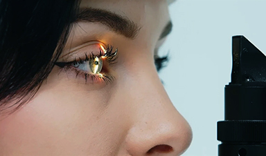
Nanomaterials in Ophthalmology: A Review
Eye diseases are becoming more common. In 2020, over 250 million people had mild vision problems, and 295 million experienced moderate to severe ocular conditions. In response, researchers are turning to nanotechnology and nanomaterials—tools that are transforming [...]

Natural Plant Extract Removes up to 90% of Microplastics From Water
Researchers found that natural polymers derived from okra and fenugreek are highly effective at removing microplastics from water. The same sticky substances that make okra slimy and give fenugreek its gel-like texture could help [...]
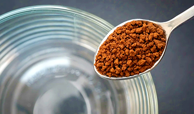
Instant coffee may damage your eyes, genetic study finds
A new genetic study shows that just one extra cup of instant coffee a day could significantly increase your risk of developing dry AMD, shedding fresh light on how our daily beverage choices may [...]
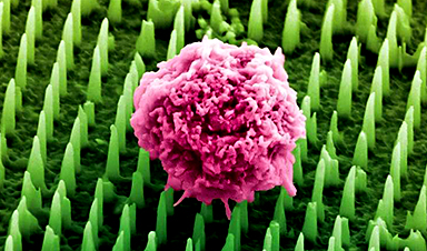
Nanoneedle patch offers painless alternative to traditional cancer biopsies
A patch containing tens of millions of microscopic nanoneedles could soon replace traditional biopsies, scientists have found. The patch offers a painless and less invasive alternative for millions of patients worldwide who undergo biopsies [...]