The development of a 3D nanoprinting platform that allows the printing of polymer materials with remarkable control and nanometer spatial accuracy is the subject of a new study published in the journal Nature Communications.
Three-dimensional (3D) printing is a layer-by-layer processing technique that has found applications in a variety of fields, including tissue printing, aviation, and product engineering. To make use of the benefits of 3D printing at the micro and nanoscale, numerous approaches for downscaling 3D printing have been established during the last few decades.
Challenges Associated with 3D Nanoprinting
There has been a widespread interest in 3D printing items at the nanometer as it enables applications where specific functional features develop at the nanoscale.
Although 3D printing has modernized industrial production and development, its application to the fabrication of polymeric nanoscale materials remains a considerable issue, owing to the challenges associated with delivering the small quantities of material with high accuracy.
An effective and reliable 3D nanoprinting system must address many critical design variables, including significant spatial control over the deposition process, constant printing with few to no intermediate steps, and solvent-free material deposition to eliminate or minimize shrinking.
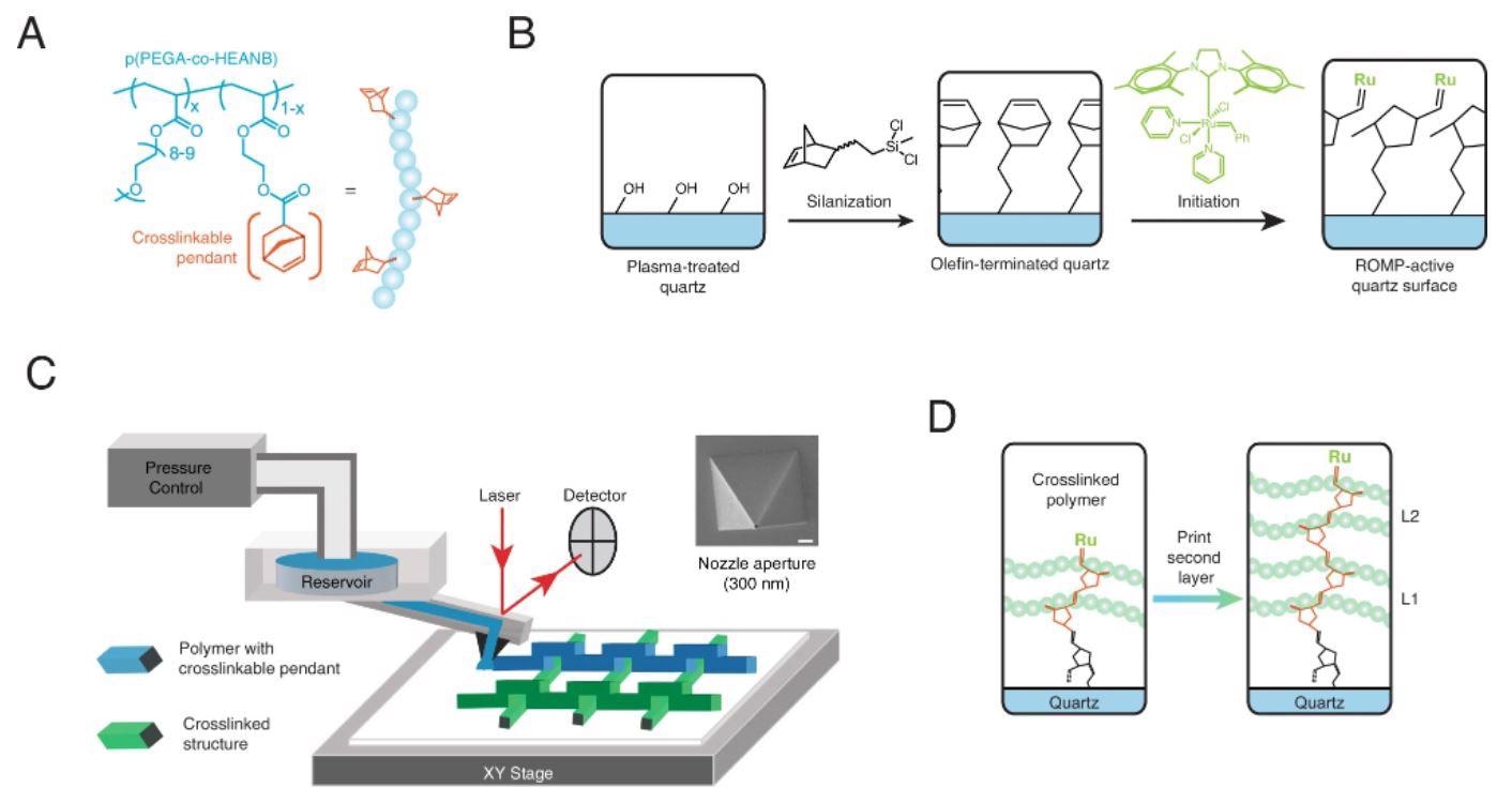
Schematic diagrams illustrating key steps in our 3D nanoprinting, including chemical crosslinking ink, surface modification and initiation, and the delivery of reactive ink to substrates to form 3D printed patterns.. A Structural formula of the crosslinking polymer, poly(polyethyleneglycol acrylate-co-hydroxyethylacrylate norbornene (p(PEGA-co-HEANB)), highlighting the crosslinkable pendant groups in orange. B Pre-functionalization of the surfaces with olefin-terminated SAM and initiated with the ROMP (ring-opening metathesis polymerization) catalyst Grubbs Generation III to enable Continuous Assembly of Polymers (CAP) upon delivery of p(PEGA-co-HEANB). C Schematic diagram illustrating the combined atomic force microscope (AFM) with microfluidic delivery, in realizing the CAP upon printing. The green material on the substrate shows crosslinked structures, while the blue is yet to be crosslinked. The inset scanning electron microscope image is of a FluidFM Nanopipette with a 300 nm aperture. Courtesy of Cytosurge AG. D Schematic of the resulting crosslinking formed after two layers of polymer have been deposited, showing the ability of the catalyst to continue crosslinking material. SEM scale bar: 2 µm. © Pattison, T. G. et al. (2022)
Development of a Novel 3D Nanoprinting Platform
In this work, researchers developed a 3D Nanoprinting technology that allows polymer materials to be printed with nanoscale spatial accuracy. The technique incorporates an atomic force microscope’s spatial precision, a microfluidic probe’s precise materials delivery, and solid-state continuous assembly and polymerization (CAP).
For nanoscale films and sheets, atomic force microscopy (AFM) is a useful characterization tool. This technology can provide high-resolution pictures and investigate local areas in both air (traditional AFM) and fluid (electrocatalytic AFM). The continuous assembly and polymerization (CAP) approach employs polymer crosslinkers with pendants, which generate highly crosslinked polymer sheets by surface-initiated polymerization (SIP) while retaining a high level of molecular flexibility due to the residual polymer side group activity.
Spatial Control and Precision of Polymer Materials
The researchers employed a combined AFM and microfluidic device to achieve spatial precision and accuracy in distributing macro crosslinkers (or polymeric inks) to the pre-functionalized substrate. The quantity of polymer supplied was regulated by changing the distribution parameters, such as pressure, velocity, and contact duration, in the microfluidic AFM platform. The AFM enabled precise movement by planning the polymeric ink’s path with nanoscale accuracy.
In contrast to previous efforts at 3D nanoprinting, this method may be used with a wide variety of polymeric composites, demonstrating great spatial precision and design accuracy owing to the quick assembly and polymerization after the distribution of the material. Furthermore, since the curing process happens at room temperature, the curing period is reduced and the material is more stable.
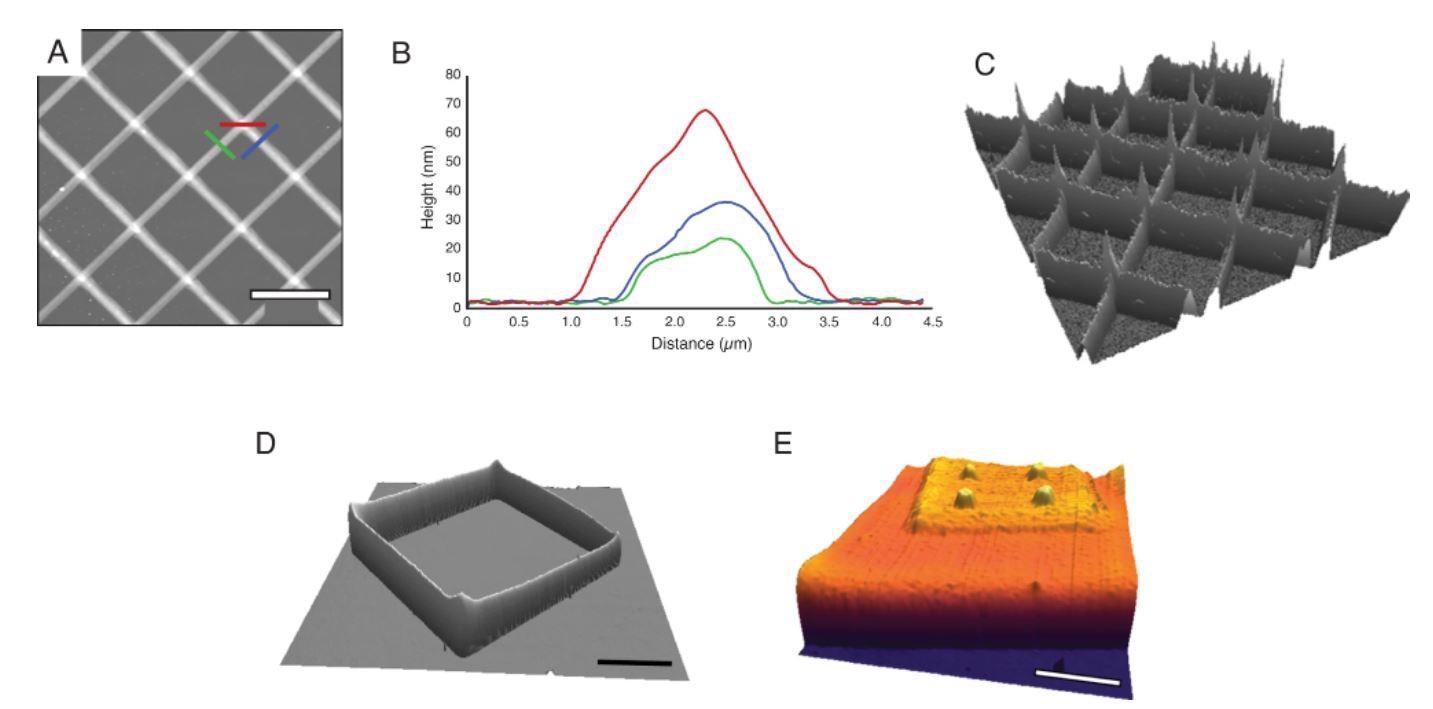
Atomic force microscopy of 3D nanoprinting following designed structures, highlighting the ability to form multilayered patterns atop of printed material. A 40 µm × 40 µm AFM topographic image of the printed cross-grids of crosslinked polymer. B Combined cursor profiles from three colored cursors indicated in A. C A 3D display of A with z scale 0–80 nm. D A 3D display of a 50 µm × 50 µm AFM topographic image of the 3D square structure with z scale 0–150 nm. E A 3D display of a 35 µm × 35 µm AFM topographic image of stacked cuboids with z scale 0–120 nm. Scale bar in A, D, and E: 10 µm. © Pattison, T. G. et al. (2022)
Important Findings of the Study
The researchers discovered that by adjusting the manufacturing settings, the breadth and height of printed materials could be readily adjusted. As the ejection rate of the polymer was almost steady under continuous reservoir pressure, the material’s height could be raised by slowing down the printing speed.
The polymeric ink was quickly cured on contact with the surface, resulting in exceptional accuracy of the 3D pattern. Because of the living nature of the linking processes, constant printing was possible without the need for additional catalysts or treatment, resulting in continuous delivery of materials in several layers. Variable print settings and complete control of the AFM-nanofluidic system were used to achieve high spatial selection and precision.
Future Perspective
In contrast to the optical-based 3D-printing techniques such as the two-photon laser process, this method allows for a broader range of applications because it can print multiple materials rather than just those containing photoconductive or photoactive substances. As a result, this technology can reduce the time necessary to manufacture compounds with photosensitive functional groups, thereby saving the overall time for 3D nanoprinting.
Future studies should concentrate on downsizing and production of overhanging components, which would need a quicker curing rate than the material delivery rate. This would enable the described 3D nanoprinting approach to be used in wearable electronics, optical systems, and biological sensors, among other applications.
News

Ebola, hantavirus: Is the world prepared for the next pandemic?
Funding cuts to health research and a growing antivaccine movement are making it harder than ever to respond to viruses. The World Health Organization (WHO) has declared that an Ebola outbreak in Uganda and [...]

May 2026 Healthcare News and Trends: Market Signals That Matter
Artificial intelligence is dominating headlines, telehealth has settled into a new normal, and digital health continues to promise transformation. However, much of what is being discussed in healthcare today reflects potential rather than reality. [...]

Scientists Rewire Donor Stem Cells To Outsmart Aggressive Blood Cancers
Researchers have tested a gene-edited stem cell transplant designed to shield healthy blood-forming cells from powerful cancer-targeting immunotherapies. For patients with highly aggressive blood cancers, stem cell transplantation can offer a rare chance at [...]

Recent Digital Health Trends, Insights and News – May 2026
Last month marked continued progress as digital health moves into its next phase — from AI expanding into drug discovery and core infrastructure to new federal pathways accelerating device access and home-based care. Together, [...]

Cancer Mystery Solved: Scientists Discover How Melanoma Becomes “Immortal”
Scientists have uncovered a previously overlooked mechanism that may help melanoma cells become effectively “immortal.” Cancer cells face a major problem before they can become deadly: They have to figure out how to stop [...]

How Visual Neurons Organize Thousands of Synaptic Inputs
Summary: A new study uncovered the organizational rules that determine how neurons in the primary visual cortex process information. By imaging both the cell bodies (soma) and the individual synapses (on dendritic spines) of [...]

Scientists Just Found a Surprising Way To Destroy “Forever Chemicals”
Scientists have uncovered a new mechanism that may help break down highly persistent PFAS pollutants. PFAS have earned the nickname “forever chemicals” for a reason. These industrial compounds are so chemically durable that they [...]

Scientists Discover Cheap Material That Kills Deadly Superbugs
A new sulfur-rich antimicrobial polymer shows strong effectiveness against fungal and bacterial pathogens and may offer an affordable solution to antimicrobial resistance. Antimicrobial resistance is creating growing challenges for both healthcare and food production, [...]

What to Know About Cicada, or BA.3.2, the Latest SARS-CoV-2 Variant Under Monitoring
Like periodical cicadas, the insects for which it is nicknamed, SARS-CoV-2 Omicron subvariant BA.3.2 is only just beginning to emerge after lying low for an extended period since it first appeared. Although it was [...]

Scientists Say This Simple Supplement May Actually Reverse Heart Disease
Scientists in Japan say a common supplement may actually help “unclog” certain diseased heart arteries from the inside out. A simple food supplement sold in Japan may have helped reverse a dangerous form of [...]

New breakthrough against radiation: Korean Scientists create revolutionary shield with nanotechnology
Korean Scientists develop new nanotechnology material capable of reducing radiation impacts in space missions, hospitals, and power plants. The search for more efficient protection technologies in extreme environments has just gained an important advance. Korean [...]

Scientists Just Discovered the Hidden Trick That Keeps Your Cells Alive
A strange bead-like motion inside cells may be the secret to keeping their DNA—and health—in balance. Mitochondria are often described as the power plants of the cell because they produce the energy cells need [...]

Scientists Discover Stem Cells That Could Regrow Teeth and Bone
Scientists just uncovered the cellular “blueprint” that could one day let us regrow real teeth. Researchers at Science Tokyo have uncovered two distinct stem cell lineages that play a central role in forming tooth [...]

Scientists Uncover Fatal Weakness in “Zombie Cells” Linked to Cancer
A newly identified weakness in “zombie” cells may open the door to more precise cancer treatments by turning their own survival strategy against them. A new class of drugs takes advantage of a recently [...]

Bowel and Ovarian Cancers Are Dramatically Rising in Young Adults, Scientists Aren’t Sure Why
Cancer incidence is increasing, especially among younger adults, and current risk factors don’t fully account for the trend. Scientists suggest other underlying causes may be contributing. Cancer patterns in England are shifting in a [...]

New Immune Pathway Could Supercharge mRNA Cancer Vaccines
A surprising backup system in the immune response to mRNA vaccines may hold the key to more effective cancer treatments. The arrival of mRNA vaccines against SARS-CoV-2 in 2020 marked a turning point in the COVID-19 pandemic. Today, [...]