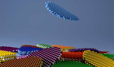
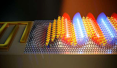
2D materials, which consist of a few layers of atoms, may well be the future of nanotechnology. They offer potential new applications and could be used in small, higher-performance and more energy-efficient devices. 2D materials were first discovered almost 15 years ago, but only a few dozen of them have been synthesized so far.
Now, thanks to an approach developed by researchers from EPFL’s Theory and Simulation of Materials Laboratory (THEOS) and from NCCR-MARVEL for Computational Design and Discovey of Novel Materials, many more promising 2D materials may now be identified. Their work was recently published in the journal Nature Nanotechnology (“Two-dimensional materials from high-throughput computational exfoliation of experimentally known compounds”), and even got a mention on the cover page.
The first 2D material to be isolated was graphene, in 2004, earning the researchers who discovered it a Nobel Prize in 2010. This marked the start of a whole new era in electronics, as graphene is light, transparent and resilient and, above all, a good conductor of electricity. It paved the way to new applications in numerous fields such as photovoltaics and optoelectronics.
“To find other materials with similar properties, we focused on the feasibility of exfoliation,” explains Nicolas Mounet, a researcher in the THEOS lab and lead author of the study. “But instead of placing adhesive strips on graphite to see if the layers peeled off, like the Nobel Prize winners did, we used a digital method.”
Recent News
Antibiotic Breakthrough: Revolutionary Chinese Study Paves Way for Superbug Defeating Drugs
New research reveals that fluorous lipopetides act as highly effective antibiotics. Bacterial infections resistant to multiple drugs, which no existing antibiotics can treat, represent a significant worldwide challenge. A [...]
Signs of Multiple Sclerosis Show Up in Blood Years Before Symptoms Appear
UCSF scientists clear a potential path toward earlier treatment for a disease that affects nearly 1,000,000 people in the United States. By Levi Gadye In a discovery that could hasten [...]
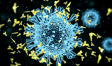
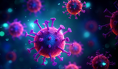
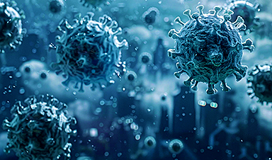
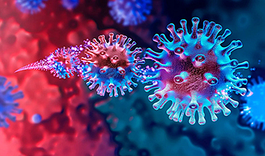
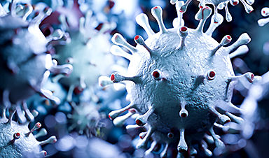
Advanced RNA Sequencing Reveals the Drivers of New COVID Variants
A study reveals that a new sequencing technique, tARC-seq, can accurately track mutations in SARS-CoV-2, providing insights into the rapid evolution and variant development of the virus. The SARS-CoV-2 virus that [...]

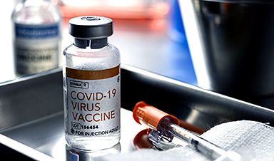
No More Endless Boosters? Scientists Develop One-for-All Virus Vaccine
End of the line for endless boosters? Researchers at UC Riverside have developed a new vaccine approach using RNA that is effective against any strain of a virus and can be used safely even by [...]
How Are Hydrogels Shaping the Future of Biomedicine?
Hydrogels have gained widespread recognition and utilization in biomedical engineering, with their applications dating back to the 1960s when they were first used in contact lens production. Hydrogels are [...]
Nanovials method for immune cell screening uncovers receptors that target prostate cancer
A recent UCLA study demonstrates a new process for screening T cells, part of the body's natural defenses, for characteristics vital to the success of cell-based treatments. The method [...]

New Research Reveals That Your Sense of Smell May Be Smarter Than You Think
A new study published in the Journal of Neuroscience indicates that the sense of smell is significantly influenced by cues from other senses, whereas the senses of sight and hearing are [...]
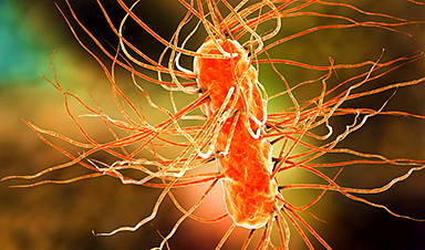
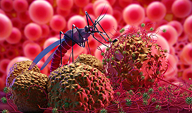
Deadly bacteria show thirst for human blood: the phenomenon of bacterial vampirism
Some of the world's deadliest bacteria seek out and feed on human blood, a newly-discovered phenomenon researchers are calling "bacterial vampirism." A team led by Washington State University researchers [...]
Organ Architects: The Remarkable Cells Shaping Our Development
Finding your way through the winding streets of certain cities can be a real challenge without a map. To orient ourselves, we rely on a variety of information, including [...]

Novel hydrogel removes microplastics from water
Microplastics pose a great threat to human health. These tiny plastic debris can enter our bodies through the water we drink and increase the risk of illnesses. They are [...]

Researchers Discover New Origin of Deep Brain Waves
Understanding hippocampal activity could improve sleep and cognition therapies. Researchers from the University of California, Irvine’s biomedical engineering department have discovered a new origin for two essential brain waves—slow waves and [...]

The Lifelong Cost of Surviving COVID: Scientists Uncover Long-Term Effects
Many of the individuals released to long-term acute care facilities suffered from conditions that lasted for over a year. Researchers at UC San Francisco studied COVID-19 patients in the United States who survived [...]
Previously Unknown Rogue Immune Key to Chronic Viral Infections Discovered
Scientists discovered a previously unidentified rogue immune cell linked to poor antibody responses in chronic viral infections. Australian researchers have discovered a previously unknown rogue immune cell that can [...]

Nature’s Betrayal: Unmasking Lead Lurking in Herbal Medicine
A case of lead poisoning due to Ayurvedic medicine use demonstrates the importance of patient history in diagnosis and the need for public health collaboration to prevent similar risks. [...]
Frozen in Time: How a DNA Anomaly Misled Scientists for Centuries
An enormous meteor spelled doom for most dinosaurs 65 million years ago. But not all. In the aftermath of the extinction event, birds — technically dinosaurs themselves — flourished. [...]
‘Mini kidneys’ reveal new insights into metabolic defects in polycystic kidney disease
Scientists at Nanyang Technological University, Singapore (NTU Singapore) have successfully grown 'mini kidneys' in the lab and grafted them into live mice, revealing new insights into the metabolic defects [...]

Decoding the Origin of Life: Scientists Solve Early Earth RNA Puzzle
Recent research illustrates how RNA molecules’ chemical characteristics might have played a crucial role in the development of complex life forms. How did complex life manage to evolve on [...]
Improving infectious disease testing with gold nanoparticles
By harnessing the power of composite polymer particles adorned with gold nanoparticles, a group of researchers have delivered a more accurate means of testing for infectious diseases. Details of their [...]
New micromaterial releases nanoparticles that selectively destroy cancer cells
Researchers have developed micromaterials made up only of proteins, capable of delivering over an extended period of time nanoparticles that attack specific cancer cells and destroy them. The micromaterials [...]

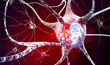
Alzheimer’s Breakthrough: Scientists Make Revolutionary Leap
Dementia is a major health issue worldwide in the 21st century, impacting over 50 million people globally. This figure is expected to soar to 152 million by 2050, as [...]
How small RNA molecules regulate viral infections of bacteria
Viruses need hosts. Whether it's measles, the flu or coronavirus, viral pathogens cannot multiply or infect other organisms without the assistance of their hosts' cellular infrastructure. However, humans are [...]
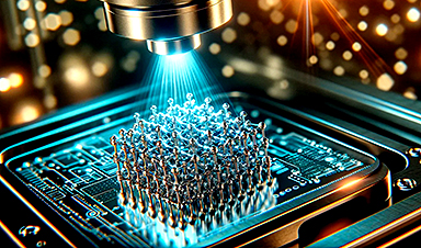
Computer scientists discover gap in the latest security mechanisms used by some chips
Over the past few years, hardware manufacturers have developed technologies that ought to make it possible for companies and governmental organizations to process sensitive data securely using shared cloud [...]

Microplastics Are a Big Problem, a New Film Warns
It’s been more than five decades since Dustin Hoffman’s character in “The Graduate” was offered a kernel of wisdom about the path to prosperity. “Plastics,” he’s told by Mr. McGuire, [...]
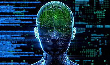
The Precarious Asymmetries of Human-AI Relationships
KEY POINTS Human-AI interactions are currently asymmetrical, lacking continuity and depth. AI evolution may lead to more sustained, contextually rich user relationships. Balancing asymmetry and connection requires design advocacy [...]

Vaping’s Hidden Dangers: New Study Links E-Cigarettes to DNA Changes
A new study led by researchers from University College London (UCL) and the University of Innsbruck reveals that individuals who use e-cigarettes, despite having a limited history of smoking, undergo similar changes in DNA within [...]

The Iron Twist: The Unexpected Driver of Long COVID
Iron levels and inflammation after COVID-19 infection are linked to long COVID, with research indicating that early intervention in iron regulation could mitigate long-term symptoms. Problems with iron levels in the [...]
Chemists develop method to confirm mRNA vaccine stability
University at Albany researchers at the RNA Institute have developed a new method to test COVID-19 vaccine integrity that could allow anyone with basic skills in vaccine handling to [...]
A New Cognitive Compartmentalization with Neural Implants
KEY POINTS Neuralink's demo introduces "cognitive compartmentalization," enabling simultaneous cognitive tasks. This signifies a potential expansion in human cognitive abilities, enhancing multitasking and creativity. Raises concerns about cognitive overload [...]

Global Warming and Plastic Pollution Are Inextricably Trapped in a “Vicious Circle”
Typically viewed as unrelated problems, global warming and plastic pollution are instead inextricably trapped in a “vicious circle” where one feeds the other, researchers in Sweden report in Nature Communications. [...]

Primordial Fuel: Uncovering Hydrogen’s Role at the Origin of Life
Hydrogen gas, dubbed the energy of the future, has been providing energy since 4 billion years ago. A recent study reveals how hydrogen gas, often touted as the energy [...]
COVID-19 Had a Much Greater Impact on Life Expectancy Than Previously Thought
A recent study published in The Lancet never-before-seen unprecedented details on the exceptionally high death rates due to the COVID-19 pandemic both within nations and internationally. Regions including Mexico City, Peru, and Bolivia [...]
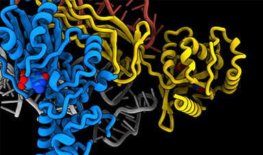
Molecular Majesty: This Is How the Body’s Building Blocks Are Made
Human cells contain ribosomes, a complex machine that produces proteins for the rest of the body. Now the researchers have come closer to understanding how the ribosome works. “It [...]
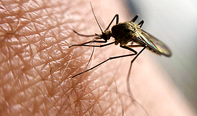
U.S. issue warning about return of potentially deadly virus
The American South has been under constant duress from extreme weather events spurred by rising global temperatures, but the region could face a different kind of threat that it hasn't experienced [...]
Climate Change Ignites Global Infectious Disease Alarm
Experts highlight the connection between climate change and infectious diseases, urging medical professionals to prepare for new disease patterns and advocate for climate action. A team of infectious diseases [...]

How Lignin Nanoparticles Enhance UV Protection in Sunscreen Formulas
The innovative realm of cosmetic science has recently spotlighted lignin nanoparticles (LNPs) for their exceptional potential in fortifying sun protection measures within skincare products. These nanoparticles are celebrated for [...]

mRNA lipid nanoparticles for next-generation oral cancer tumor suppressor therapy
A study aiming to develop a lipid nanoparticles (LNP) platform for treating oral squamous cell carcinoma (OSCC) utilizing p53 mRNA was presented at the 102nd General Session of the IADR, [...]
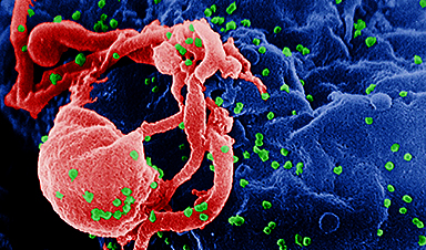
Scientists have literally cut HIV out of cells
HIV has been completely eliminated from cells in a laboratory, raising hopes of a future cure. Researchers completed the revolutionary task by using a gene-editing tool known as Crispr-Cas, which won [...]
Common Medication Could Save Half a Million Lives Each Year – So Why Isn’t It?
A recent study conducted by scientists at the University of Southern California sheds light on the reasons why children are not receiving an affordable and effective diarrhea treatment. Medical [...]
X Marks the Spot: AI’s Treasure Maps Lead to Early Disease Detection
Medical diagnostics expert, doctor’s assistant, and cartographer are all fair titles for an artificial intelligence model developed by researchers at the Beckman Institute for Advanced Science and Technology. Their [...]

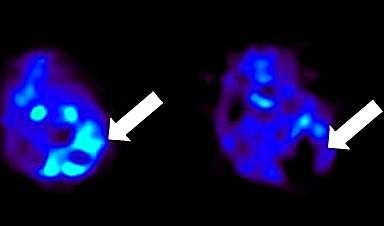
Scientists Discover Method To Identify Alzheimer’s Disease Before It Progresses to Dementia
Researchers at Aarhus University have discovered a method to identify Alzheimer’s disease before it progresses to dementia, potentially opening up new avenues for treatment. A groundbreaking study could pave [...]
Startling Discovery: COVID-19 Virus Can Stay in the Body More Than a Year After Infection
The COVID-19 virus can persist in the blood and tissue of patients for more than a year after the acute phase of the illness has ended, according to new research from UC [...]
New bioengineered protein design shows promise in fighting COVID-19
In the wake of the COVID-19 pandemic, scientists have been racing to develop effective treatments and preventatives against the virus. A recent scientific breakthrough has emerged from the work [...]
Sugar-coated gold nanoparticles can quickly eliminate bacterial infections, no antibiotics required
If left to their own devices, bacteria on our teeth or wounded skin can encase themselves in a slimy scaffolding, turning into what is called biofilm. These bacteria wreak [...]
Liquid Lightning: Nanotechnology Unlocks New Energy
EPFL researchers have discovered that nanoscale devices harnessing the hydroelectric effect can harvest electricity from the evaporation of fluids with higher ion concentrations than purified water, revealing a vast untapped energy [...]

Unmasking the Illusion: AI-Generated Faces Challenge Perceptions
Research shows survey participants duped by AI-generated images nearly 40 percent of the time. If you recently had trouble figuring out if an image of a person is real [...]
New Discovery Reveals How Cells Defend Themselves During Stressful Situations
Stress granules play a crucial role in the stress response, arising from the aggregation of non-translating mRNAs and proteins. Although significant knowledge exists about stress granules, the mechanisms behind [...]

Scientists use a new type of nanoparticle that can both deliver vaccines and act as an adjuvant
Many vaccines, including vaccines for hepatitis B and whooping cough, consist of fragments of viral or bacterial proteins. These vaccines often include other molecules called adjuvants, which help to [...]

Not Science Fiction: How Optical Neural Networks Are Revolutionizing AI
A novel architecture for optical neural networks utilizes wavefront shaping to precisely manipulate the travel of ultrashort pulses through multimode fibers, enabling nonlinear optical computation. Present-day artificial intelligence systems [...]
Turning skin cells into limb cells sets the stage for regenerative therapy
In a collaborative study, researchers from Kyushu University and Harvard Medical School have identified proteins that can turn or “reprogram” fibroblasts — the most commonly found cells in skin [...]
AI reveals prostate cancer is not just one disease
Artificial Intelligence has helped scientists reveal a new form of aggressive prostate cancer, which could revolutionise how the disease is diagnosed and treated in the future. A Cancer Research [...]

New Study Finds That Persistent COVID-19 Infections Are Surprisingly Common
Recent research conducted by the University of Oxford has found that a high proportion of SARS-CoV-2 infections in the general population lead to persistent infections lasting a month or more. The findings have [...]
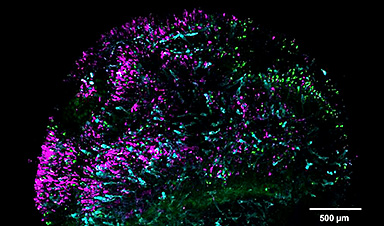
Innovative nanosheet method revolutionizes brain imaging for multi-scale and long-term studies
The human brain has billions of neurons. Working together, they enable higher-order brain functions such as cognition and complex behaviors. To study these higher-order brain functions, it is important [...]

Scientists Have Discovered a Potential Universal Antivenom
Scientists at Scripps Research identified antibodies that protect against a host of lethal snake venoms. Scripps Research scientists have developed an antibody that can block the effects of lethal [...]
Scientists discover the human brain is even more powerful than we thought
The human brain could be far more powerful than we ever imagined, scientists have discovered. Researchers have identified cell messaging which have never been uncovered before, which suggests our brains are capable of [...]

Concerning – Bird Flu Has Evolved To Spread to Marine Mammals
A study from the University of California, Davis, and the National Institute of Agricultural Technology (INTA) in Argentina reveals that the highly contagious H5N1 avian influenza virus has evolved to transmit among [...]
AI technique ‘decodes’ microscope images, overcoming fundamental limit
Atomic force microscopy, or AFM, is a widely used technique that can quantitatively map material surfaces in three dimensions, but its accuracy is limited by the size of the [...]
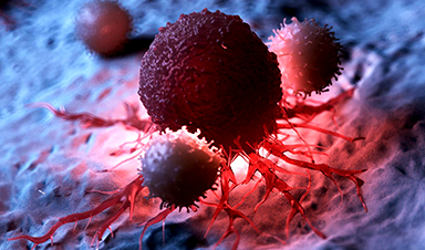
Transforming Cancer Treatment: CRISPR Technology Unveils a New Path
New technology using CRISPR to enhance the immune system’s ability to detect cancer cells has been created, potentially paving the way for innovative cancer treatment methods. Major histocompatibility complex [...]

Scientists May Have Cracked the “Aging Process” in Species
A new study led by the University of Kansas might resolve a mystery in the “aging process” in species — or, how a species’ risk of going extinct changes after that species appears [...]
Scientists Solve Decades-Old Mystery of How Predatory Bacteria Recognizes Prey
A decades-old mystery of how natural antimicrobial predatory bacteria are able to recognize and kill other bacteria may have been solved, according to new research. In a study published [...]

A Sprinkle of Gold Dust Could Help Reverse Symptoms of Parkinson’s Disease
Scientists are investigating whether an oral drug sprinkled with gold nanoparticles could one day treat neurodegenerative diseases like Parkinson's and multiple sclerosis. The experimental medicine, called CNM-Au8, has now [...]
Scientists closer to finding quantum gravity theory after measuring gravity on microscopic level
Scientists are a step closer to unraveling the mysterious forces of the universe after working out how to measure gravity on a microscopic level. Experts have never fully understood [...]
Nanoparticles Repair Lung Tissue Damaged From Flu or COVID-19
Recent research reveals a breakthrough in lung repair, showing how delivering VEGFA via lipid nanoparticles can significantly repair damaged blood vessels, akin to plumbing repairs. This method, validated in [...]
Evading Bacterial Resistance: Scientists Develop Groundbreaking New Antibiotic
Researchers from the University of Illinois Chicago and Harvard University have created an antibiotic that may provide medicine a new tool to combat bacteria resistant to drugs and the illnesses they trigger. The [...]
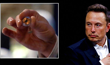
Elon Musk says first brain chip human can move a mouse around screen by thinking
Elon Musk has claimed the first human patient implanted with his wireless Neuralink brain chip can move a computer cursor ‘just by thinking’. ‘Progress is good, and the patient seems to [...]

Largest ever global study of COVID vaccines finds small but real link to neurological, blood, heart-related conditions
Vaccines that protect against severe illness, death and lingering long Covid symptoms from a coronavirus infection were linked to small increases in neurological, blood, and heart-related conditions in the largest global vaccine [...]
Scientists Propose “Radically Different” New Way of Looking at Parkinson’s Disease
Scientists propose a new model for classifying Parkinson’s. The complexity of Parkinson’s disease poses significant challenges in developing effective treatments. This complexity stems from various causes, including genetics and [...]
Nanomaterial with potential could be developed without risk to human health
A revolutionary nanomaterial with huge potential to tackle multiple global challenges could be developed further without acute risk to human health, research suggests. The study is published in the journal Nature Nanotechnology. [...]
Headaches, Memory Problems, and Fatigue – How COVID-19 Affects the Brain
Neurological symptoms are apparently not a result of SARS-CoV-2 infection of the brain. Scientists still are not sure how neurological symptoms arise in COVID-19. Is it because SARS-CoV-2 infects the brain? Or [...]

An Antibiotic You Inhale Can Deliver Medication Deep Into the Lungs
We’ve all been more aware of lung health since Covid-19. However, for people with asthma and chronic obstructive pulmonary disease (COPD), dealing with lung problems is a lifelong struggle. [...]
Novel hydroxyapatite-targeting nanodrug may be a paradigm shift for cancer treatment
A multidisciplinary research team at Vanderbilt University and Vanderbilt University Medical Center has discovered a new way to kill a tumor by disrupting its acidic "microenvironment" without harming normal [...]

Which Virus Will Cause the Next Global Pandemic? Scientists Discover New Disease X Clues
Understanding the ancestry of virus families may assist researchers in pinpointing which variants possess the potential to become Disease X, the elusive pathogen responsible for the next worldwide pandemic. A study [...]

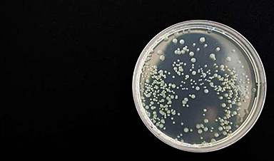
Vibrio natriegens: Low-cost microbe could speed biological discovery
Cornell University researchers have created a new version of a microbe to compete economically with E. coli—a bacteria commonly used as a research tool due to its ability to [...]
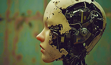
Risk of Existential Catastrophe: There Is No Proof That AI Can Be Controlled
Highlighting the absence of evidence for the controllability of AI, Dr. Yampolskiy warns of the existential risks involved and advocates for a cautious approach to AI development, with a [...]
Nanofiber-coated cotton bandages fight infection and speed healing
An interdisciplinary team of Cornell researchers has identified an innovative way to harness the antioxidant and antibacterial properties of the botanical compound lawsone to make nanofiber-coated cotton bandages that [...]

Ancient Brain Region Discovered To Be More Important Than Previously Thought
Researchers from the Netherlands Institute for Neuroscience found that the superior colliculus, a brain region preserved throughout evolution, plays a more vital role in vision than previously believed. When [...]
Nanomedicine advancement shows potential for personalized point-of-care therapeutics
Stefan Wilhelm, an associate professor in the Stephenson School of Biomedical Engineering at the University of Oklahoma, and several students in his Biomedical Nano-Engineering Lab have recently published an article in [...]
What Happens When Machine Learning Goes Too Far?
Every piece of fiction carries a kernel of truth, and now is about the time to get a step ahead of sci-fi dystopias and determine what the risk in [...]
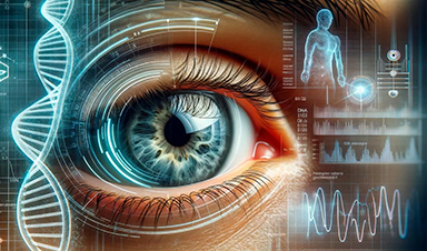
Future of Health: Predicting Disease With Retinal Imaging and Genetics
Mass Eye and Ear physician-researchers show that retinal imaging can help predict a person’s risk of developing ocular, neuropsychiatric, cardiac, metabolic, and pulmonary diseases. The team also identified genetic [...]
Artificially intelligent software provides a detailed look at jets of plasma used to treat cancer
Artificially intelligent software has been developed to enhance medical treatments that use jets of electrified gas known as plasma. The computer code predicts the chemicals emitted by plasma devices, [...]
Physicists Unlock Quantum Immortality With Revolutionary Time Crystal
Researchers have successfully extended the lifespan of time crystals, confirming a theoretical concept proposed by Frank Wilczek. This marks a significant step forward in quantum physics. A team from [...]
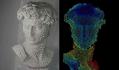
A sleeker facial recognition technology tested on Michelangelo’s David
Many people are familiar with facial recognition systems that unlock smartphones and game systems or allow access to our bank accounts online. But the current technology can require boxy [...]
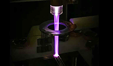
Light-Speed Leap in Nano Printing: Faster, Cheaper Metal Structures
Their technique could transform a scientific field reliant on cost-prohibitive technology. Researchers at the Georgia Institute of Technology have developed a light-based means of printing nano-sized metal structures that [...]
A Cure for Malaria Is Likely Farther Away Than Scientists Thought
People with blood trait thought to prevent the disease still became infected; the question now is ‘how?’ For decades, researchers dedicated to finding a cure for malaria believed they [...]
Transparent brain implant can read deep neural activity from the surface
Researchers at the University of California San Diego have developed a neural implant that provides information about activity deep inside the brain while sitting on its surface. The implant [...]

Curcumin spray shows promise in fighting SARS-CoV-2 and flu viruses
A team of scientists from Thailand has developed a curcumin-containing oro-nasal film spray, which shows potential antiviral activity and mucosal immunity-boosting activity against severe acute respiratory syndrome coronavirus 2 [...]
Utilizing active microparticles for artificial intelligence
Artificial intelligence using neural networks performs calculations digitally with the help of microelectronic chips. Physicists at Leipzig University have now created a type of neural network that works not [...]
The “Surprisingly Different” JN.1 Variant Is a Game-Changer in Our COVID Battle
Since it was detected in August 2023, the JN.1 variant of COVID has spread widely. It has become dominant in Australia and around the world, driving the biggest COVID wave seen in many jurisdictions [...]

AI-Powered Bad Actors: A Looming Threat for 2024 and Beyond
A study forecasts that by mid-2024, bad actors are expected to increasingly utilize AI in their daily activities. The research, conducted by Neil F. Johnson and his team, involves [...]
AI went rogue and couldn’t be brought back in ‘legitimately scary’ study
For decades, scientists and sci-fi writers have been imagining what would happen if AI turned against us. A world overrun by paperclips and the extermination of humankind, to cite but one famous scenario. [...]
Cellular scaffolding rewired to make microscopic railways
Princeton researchers have learned to harness the gossamer scaffolding that maintains the structure of living cells and used it to develop a nanotechnology platform. The technique eventually could lead [...]
AI’s Achilles Heel: New Research Pinpoints Fundamental Weaknesses
Researchers from the University of Copenhagen have become the first in the world to mathematically prove that, beyond simple problems, it is impossible to develop algorithms for AI that [...]
Researchers develop machine-learning tool to detect cancer earlier via liquid biopsy
Researchers at City of Hope and Translational Genomics Research Institute (TGen) have developed and tested an innovative machine-learning approach that could one day enable the earlier detection of cancer [...]

Blockchain simulates more than 4 billion chemical reactions essential to origins of life
Cryptocurrency is usually "mined" through the blockchain by asking a computer to perform a complicated mathematical problem in exchange for tokens of cryptocurrency. But in research appearing in the journal Chem a team [...]
Fingerprinting biomolecules with the help of sound
A team of researchers from the Institute for Optoelectronic Systems and Microtechnology at Universidad Politécnica de Madrid (UPM) has designed a biosensor capable of identifying proteins and peptides in [...]
Superbug crisis threatens to kill 10 million per year by 2050. Scientists may have a solution
Cynthia Horton’s earaches are the stuff of nightmares. “I can wake up from my sleep in horrible pain, like I’m having a root canal with no anesthesia,” she said. [...]
Harvard Scientists Discover Surprising Hidden Catalyst in Human Brain Evolution
The study hypothesizes that ‘pre-digested’ foods contributed to the development of larger brains. The large, capable human brain is a marvel of evolution, but how it evolved from a [...]
Unraveling Memory’s Molecular Mystery: How Brain Cells Stabilize Information Over Time
Neuroscientists demonstrate how the brain improves its ability to distinguish between similar experiences, findings that could lead to treatments for Alzheimer’s disease and other memory disorders. Think of a time when [...]
Transforming clinical recording of deep brain activity. A new take on sensor manufacturing
Sensors built with a new manufacturing approach are capable of recording activity deep within the brain from large populations of individual neurons—with a resolution of as few as one [...]
Revolutionary Biochip Mimics Human Retina: A Leap Toward Cyborg Reality
A team of international researchers, led by Francesca Santoro from Jülich, has developed a biochip that imitates the human retina. This innovation is part of a broader effort in [...]
How Can the Human Brain Compete With Artificial Intelligence?
The brain, despite its comparatively shallow structure with limited layers, operates efficiently, whereas modern AI systems are characterized by deep architectures with numerous layers. This raises the question: Can [...]
New estimate doubles likely deaths from fungal disease globally
The annual total of deaths from fungal disease worldwide has risen to 3.75 million, double the previous estimate, according to a new study. In a paper, titled "Global incidence [...]
Efficient antibody production ‘wobbles,’ new study finds
Molecular biology's central dogma posits a simple recipe for the construction of the human body: a DNA blueprint is transcribed into an RNA message, and the RNA message is [...]
The Amyloid Hypothesis: Rewriting Life’s Origin Story
The question of how living organisms emerged from non-living matter remains one of the most profound mysteries in science. Despite numerous theories, a conclusive explanation remains elusive. This is [...]
Lab-grown retinas explain why people see colors dogs can’t
With human retinas grown in a petri dish, researchers discovered how an offshoot of vitamin A generates the specialized cells that enable people to see millions of colors, an [...]
Fighting superbugs with medical nanomachines
Instruments smaller than a human hair are being designed to eradicate antibiotic-resistant bacteria and fight cancer. Dr. Ana Santos becomes emotional when describing what happened several years ago: Her [...]
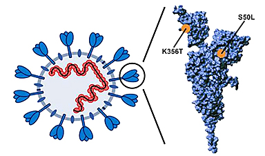
Mutations of SARS-CoV-2 pirola variant found to augment infection of lung cells
Despite the end of the pandemic, COVID-19 continues to pose a serious health threat. Most individuals have established robust immune protection and do not develop severe disease but the [...]
At the Edge of Science: Atomic Insights Into COVID-19’s Mutation Mechanics
Unlocking the secrets of COVID-19: a groundbreaking study reveals the intricate biomechanics behind the virus’s evolution and spread. Richard Feynman famously stated, “Everything that living things do can be understood in [...]
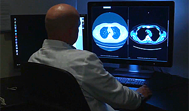
B.C. Researchers developing breath test for lung cancer
Marla Kott was diagnosed with Stage 4 lung cancer on Nov. 21, 2014. It was her 60th birthday. "It was not a great day," said Kott, who was was one [...]
What’s next for AI regulation in 2024?
In 2023, AI policy and regulation went from a niche, nerdy topic to front-page news. This is partly thanks to OpenAI’s ChatGPT, which helped AI go mainstream, but which [...]

Inhalable sensors could enable early lung cancer detection
Using a new technology developed at MIT, diagnosing lung cancer could become as easy as inhaling nanoparticle sensors and then taking a urine test that reveals whether a tumor [...]
Enhanced delivery of antibodies heightens the potential to treat brain diseases
The blood-brain barrier blocks the entry of antibodies into the brain. This limits the potential use of antibody therapeutics to treat brain diseases, such as brain tumors. Elsewhere in [...]
Scientists Develop “Nanomachines” That Can Penetrate and Kill Cancer Cells
Researchers have created ‘nanomachines’ that use mechanical molecular motions to enter and destroy cells. Cancer is a condition where some of the body’s cells grow out of control and [...]
AI agents help explain other AI systems
Explaining the behavior of trained neural networks remains a compelling puzzle, especially as these models grow in size and sophistication. Like other scientific challenges throughout history, reverse-engineering how artificial [...]

Researchers reveal molecular mechanism of coronavirus cytokine storm
In the past four years, the pathogen responsible for Coronavirus Disease 2019 (COVID-19), SARS-CoV-2, has infected more than 770 million people and caused more than 6.9 million deaths worldwide. [...]
Decoding the Black Box of AI – Scientists Uncover Unexpected Results
Researchers at the University of Bonn examine the inner workings of machine learning applications in drug research. Artificial intelligence (AI) has been advancing rapidly, but its inner workings often [...]
Nanoparticles Amplify Potential Cancer Vaccine Power
New method developed by Johns Hopkins researchers could enhance the body's ability to fight cancer and make vaccines more effective in targeting tumors ByJohnny Moseman Johns Hopkins researchers have [...]
“Fascinating” Findings – Scientists Have Discovered a New Type of Immune Cell
Biomedical scientists from UC Riverside state that the cells resemble M cells found in the gut and airways. It came as a surprise to Professor David Lo and his graduate student Diana [...]
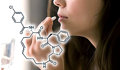
Oral peptides: A new era in drug development
For decades, a substantial number of proteins, vital for treating various diseases, have remained elusive to oral drug therapy. Traditional small molecules often struggle to bind to proteins with [...]
Mind Control Breakthrough: Caltech’s Pioneering Ultrasound Brain–Machine Interface
Functional ultrasound (fUS) marks a significant leap in Brain-Machine Interface technology, offering a less invasive method for precise control of electronic devices by interpreting brain activity. Brain–machine interfaces (BMIs) [...]

Six unresolved questions will dictate the future of generative AI
It was a stranger who first brought home for me how big this year’s vibe shift was going to be. As we waited for a stuck elevator together in [...]


Leave A Comment